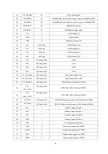
- -
45
10
D4
I/O Pull up
Flash/ LCD/ SDRAM data bus bit 4
11
D5
I/O Pull up
Flash/ LCD/ SDRAM data bus bit 5
12
D6
I/O Pull up
Flash/ LCD/ SDRAM data bus bit 6
13
D7
I/O Pull up
Flash/ LCD/ SDRAM data bus bit 7
14
RD/BY
I, Pull up
Flash ready/busy signal
15
FREN
O
Flash read enable
16
FWEN
O
Flash write enable
17
FWP
O
Flash write protect
18
VDD
P
Digital Core power(1.8V)
19
VSSD
P
Digital Core Ground
20
VCC
P
I/O POWER(3.3V)
21
P2.4/A0
I/O
SDRAM/ SRAM Address Bit 0
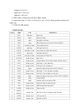
,
GPIO
22
P2.5/A1
I/O
SDRAM/ SRAM Address Bit 1 GPIO; FALE/LCDRS
23
P2.6/A2
I/O
SDRAM/ SRAM Address Bit 2 GPIO; FCLE
24
P2.7/A3
I/O
SDRAM/ SRAM Address Bit 3
,
GPIO
25
A4
O
SDRAM/ SRAM Address Bit 4
26
A5
O
SDRAM/ SRAM Address Bit 5
27
A6
O
SDRAM/ SRAM Address Bit 6
28
A7
O
SDRAM/ SRAM Address Bit 7
29
A8
O
SDRAM/ SRAM Address Bit 8
30
A9
O
SDRAM/ SRAM Address Bit 9
31
A10
O
SDRAM Address Bit 10
32
A11
O
SDRAM Address Bit 11 SRAM Address Bit 10
33
A12
O
SDRAM Address Bit 12 SRAM Address Bit 11
34
BA0
O
SDRAM Bank Address 0 SRAM Address Bit 12
35
BA1
O
SDRAM Bank Address 1 SRAM Address Bit 13
36
CKE
O
SDRAM clock enable to SDRAM
37
CLK
O
system clock to SDRAM
38
P2.8/WEN
I/O
SDRAM write enable GPIO
39
P2.9/CASN
I/O
SDRAM column address strobe GPIO
40
P2.10/RASN
I/O
SDRAM row address strobe GPIO
41
P2.11/CSN
I/O
SDRAM chip strobe GPIO
42
VSSD
P
Digital Ground


