- -
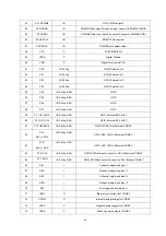
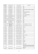
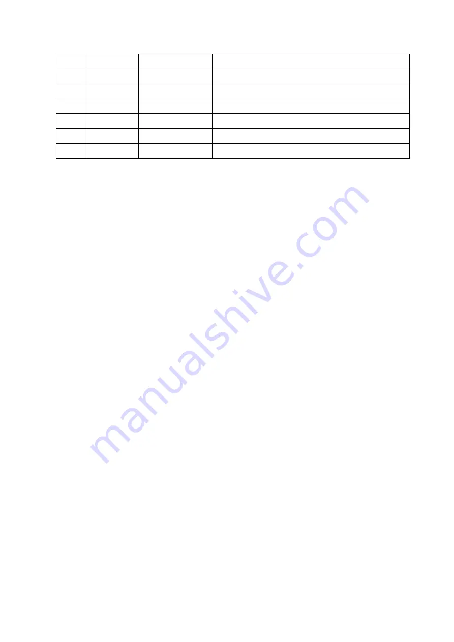
57
26
LINPUT2
Analogue Input
Left Channel Input 2
27
RINPUT1
Analogue Input
Right Channel Input 1
28
LINPUT1
Analogue Input
Left Channel Input 1
29
MODE
Digital Input
Control Interface Selection
30
CSB
Digital Input
Chip Select / Device Address Selection
31
SDIN
Digital Input/Output
Control Interface Data Input / 2-wire Acknowledge output
32
SCLK
Digital Input
Control Interface Clock Input
3.5.9 Function introduction to XC6206P152MR
1. Description
The XC6206 series are highly precise, low power consumption, high voltage, positive voltage
regulators manufactured using CMOS and laser trimming technologies. The series provides large currents
with a significantly small dropout voltage.
The XC6206 consists of a current limiter circuit, a driver transistor, a precision reference voltage and
an error correction circuit.
The series is compatible with low ESR ceramic capacitors. The current limiter's foldback circuit also
operates as a short protect for the output current limiter and the output pin.
Output voltage can be set internally by laser trimming technologies. It is selectable in 0.1V increments
within a range of 1.2V to 5.0V.
SOT-23 (250mW) and SOT-89 (500mW) packages are available.
2. Features
◆
Maximum Output Current : 250mA (5.0V type)
◆
Dropout Voltage : 160mV @ 100mA (5.0V type)
◆
Maximum Operating Voltage : 6.0V
◆
Output Voltage Range : 1.2V ~ 5.0V (selectable in 0.1V steps)
◆
Highly Accurate : ± 2%
◆
Low Power Consumption : Typ. 1.0µA
◆
Operational Temperature Range : -40OC ~ 85OC
◆
Ultra Small Packages : SOT-23 (250mW), SOT-89 (500mW)
◆
Low ESR Capacitor : Ceramic compatible


