background image

Chapter:

 Connectors 

Mini-PCI 

page 22 

Beckhoff New Automation Technology 

CB2051


3.5  Mini-PCI 

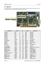
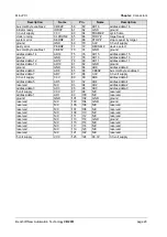
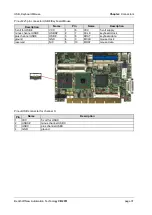
The CB2051 allows you to add expansion cards complying to the Mini-PCI standard (type III). One such 
card can be inserted into the Mini-PCI slot available on the board. 


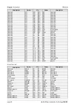
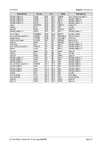
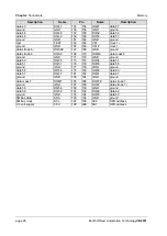
Description 

Name 

Pin 

Name 

Description 

reserved 

N/C 

N/C 

reserved 

reserved 

N/C 

N/C 

reserved 

reserved 

N/C 

N/C 

reserved 

reserved 

N/C 

N/C 

reserved 

reserved 

N/C 

10 

N/C 

reserved 

reserved 

N/C 

11 

12 

N/C 

reserved 

reserved 

N/C 

13 

14 

N/C 

reserved 

reserved 

N/C 

15 

16 

N/C 

reserved 

interrupt B 

INTB# 

17 

18 

VCC 

5 volt supply 

3.3 volt supply 

3.3V 

19 

20 

INTA# 

interrupt A 

reserved 

N/C 

21 

22 

N/C 

reserved 

ground 

GND 

23 

24 

S3.3V 

3.3 volt supply 

PCI clock 

PCLK 

25 

26 

PRST# 

reset 

ground 

GND 

27 

28 

3.3V 

3.3 volt supply 

PCI request 

REQ# 

29 

30 

GNT# 

PCI grant 

3.3 volt supply 

3.3V 

31 

32 

GND 

ground 

address/data 31 

AD31 

33 

34 

PME# 

power management event 

address/data 29 

AD29 

35 

36 

N/C 

reserved 

ground 

GND 

37 

38 

AD30 

address/data 30 

address/data 27 

AD27 

39 

40 

3.3V 

3.3 volt supply 

address/data 25 

AD25 

41 

42 

AD28 

address/data 28 

reserved 

N/C 

43 

44 

AD26 

address/data 26 

bus cmd/byte enables 3 

CBE3# 

45 

46 

AD24 

address/data 24 

address/data 23 

AD23 

47 

48 

IDSEL 

init device select 

ground 

GND 

49 

50 

GND 

ground 

address/data 21 

AD21 

51 

52 

AD22 

address/data 22 

address/data 19 

AD19 

53 

54 

AD20 

address/data 20 

ground 

GND 

55 

56 

PAR 

parity 

address/data 17 

AD17 

57 

58 

AD18 

address/data 18 

Summary of Contents for CB2051

Page 1: ...Beckhoff Automation GmbH phone 49 0 52 46 963 0 Eiserstr 5 fax 49 0 52 46 963 198 33415 Verl email info beckhoff de Germany web www beckhoff de CB2051 Manual rev 1 3 ...

Page 2: ......

Page 3: ... 1 Features 12 2 2 Specifications and Documents 14 3 Connectors 15 3 1 Power Supply 16 3 2 CMOS Battery 17 3 3 System 18 3 4 PISA Slot 19 3 5 Mini PCI 22 3 6 Memory 24 3 7 SATA Interfaces 27 3 8 IDE interface 28 3 9 Floppy interface 29 3 10 USB Keyboard Mouse 30 3 11 Serial Interfaces COM1 COM2 32 3 12 Serial Interfaces COM3 COM4 33 3 13 VGA DVI 34 3 14 LVDS 35 3 15 LAN1 37 3 16 LAN2 38 3 17 Touch...

Page 4: ... Fail Safe Defaults 68 4 12 Load Optimized Defaults 68 4 13 Set Password 68 4 14 Save Exit Setup 68 4 15 Exit Without Saving 68 5 BIOS update 69 6 Mechanical Drawings 70 6 1 PCB Mounting Holes 70 6 2 PCB Pin1 Dimensions 71 6 3 PCB Die Center 72 7 Technical Data 73 7 1 Electrical Data 73 7 2 Environmental Conditions 73 7 3 Thermal Specifications 74 8 Support and Service 75 8 1 Beckhoff s Branch Off...

Page 5: ...Notes on the Documentation Chapter Document History Beckhoff New Automation Technology CB2051 page 5 ...

Page 6: ... updated contact details minor changes 1 1 minor changes 1 2 improved print quality of dimensional drawings minor changes 1 3 updated LAN pinout in chapter 3 16 Annex II added Gameport NOTE All company names brand names and product names referred to in this manual are registered or unregistered trademarks of their respective holders and are as such protected by national and international law ...

Page 7: ...d are however constantly under development For that reason the documentation is not in every case checked for consistency with performance data standards or other characteristics None of the statements of this manual represents a guarantee Garantie in the meaning of 443 BGB of the German Civil Code or a statement about the contractually expected fitness for a particular purpose in the meaning of 4...

Page 8: ...instructions are to be found on the following pages or in the areas mounting wiring commissioning etc 1 2 1 Disclaimer All the components are supplied in particular hardware and software configurations appropriate for the application Modifications to hardware or software configurations other than those described in the documentation are not permitted and nullify the liability of Beckhoff Automatio...

Page 9: ...o the safety advise next to this symbol there is immediate danger to life and health of individuals RISK OF INJURY If you do not adhere to the safety advise next to this symbol there is danger to life and health of individuals HAZARD TO INDIVIDUALS ENVIRONMENT DEVICES OR DATA If you do not adhere to the safety advise next to this symbol there is obvious hazard to individuals to environment to mate...

Page 10: ...nal safety and environmental protection aspects o the operating personnel is familiar with the operating manual and in particular the safety notes contained herein 1 3 2 National Regulations Depending on the Machine Type Depending on the type of machine and plant in which the product is used national regulations governing the controllers of such machines will apply and must be observed by the oper...

Page 11: ... Automation GmbH this product description shall be applied only in limited scope Only the contractually agreed specifications of the corresponding Industrial PC from Beckhoff Automation GmbH shall be relevant Due to several models of Industrial PCs variations in the component placement of the motherboards are possible Support and service benefits for the built in motherboard will be rendered by Be...

Page 12: ...CD connectors o Processor Intel Celeron M Intel Core Duo or Intel Core 2 Duo o Chipset Intel 945GM and Intel ICH7 o Two SO DIMM200 slots for up to 2 GByte DDR2 667 o Four serial ports COM1 to COM4 o LAN Ethernet 10 100 Base T o LAN Ethernet 10 100 1000 Base T o Two SATA channels o IDE interface o PS2 keyboard mouse interface o Floppy interface o Eight USB 2 0 interfaces o AWARD BIOS 6 10 o CRT int...

Page 13: ...utomation Technology CB2051 page 13 o TFT interface via LVDS 18 Bit o AC97 compatible sound including SPDIF in and output o RTC with external CMOS battery o MiniPCI slot o PCI bus via PISA slot connector o 16x GPIO o Format 192 mm x 125 5 mm ...

Page 14: ...I Specification Version 3 0 www acpi info ATA ATAPI Specification Version 7 Rev 1 www t13 org USB Specifications www usb org SM Bus Specification Version 2 0 www smbus org Intel Chipset Description Mobile Intel 945 Express Chipset Family Datasheet www intel com Intel Chip Description ICH7 Datasheet www intel com Intel Chip Descriptions Celeron M Core Duo Solo Core2 Duo www intel com Winbond Chip D...

Page 15: ...CB2051 CAUTION For most interfaces the cables must meet certain requirements For instance USB 2 0 requires twisted and shielded cables to reliably maintain full speed data rates Restrictions on maximum cable length are also in place for many high speed interfaces and for power supply Please refer to the respective specifications and use suitable cables at all times ...

Page 16: ...talled these pins have no function COM3 RXD and TXD can also be used for connecting a second power supply unit e g for UPS As an ordering option SMBus signals SCL SDA can be provided replacing COM3 TXD RXD Description Name Pin Name Description COM3 transmit data TXD 1 9 RXD COM3 receive data PSU on PS ON 2 10 PWRGD Powergood powerbutton PSU PWRBTN 3 11 SVCC standby supply 5V 12 volt supply 12V 4 1...

Page 17: ...051 page 17 3 2 CMOS Battery The board ships with a CR2032 battery holder Renata VBH2032 1 and 3V battery Alternatively an external battery can be connected via a 2pin connector JST B2B EH A mating connector EHR 2 Pin Name Description 1 BATT battery 3 3 volt 2 GND ground ...

Page 18: ...D2 are already provided with a series resistor As can be seen from the pinout table below corresponding signals are often placed vis à vis or at least near to each other Description Name Pin Name Description ground GND 1 10 PWRBTN on suspend button ground GND 2 11 RESET reset to ground LED touch screen TOUCHLED 3 12 3 3V 3 3 volt supply LED suspend ACPI S LED 4 13 S3 3V standby supply 3 3 volt LED...

Page 19: ...through D while the latter is divided into segments E through H cf the illustration above Pinout up row Description Name Pin Name Description reserved N C A1 B1 GND ground reserved N C A2 B2 N C reserved reserved N C A3 B3 VCC 5 volt supply reserved N C A4 B4 N C reserved reserved N C A5 B5 5V 5 volt supply reserved N C A6 B6 N C reserved reserved N C A7 B7 12V 12 volt supply reserved N C A8 B8 N ...

Page 20: ...eserved N C C10 D10 N C reserved reserved N C C11 D11 N C reserved reserved N C C12 D12 N C reserved reserved N C C13 D13 N C reserved reserved N C C14 D14 N C reserved reserved N C C15 D15 N C reserved reserved N C C16 D16 VCC 5 volt supply reserved N C C17 D17 N C reserved reserved N C C18 D18 GND ground Pinout low row Description Name Pin Name Description I2C clock I2CLK E1 F1 I2DAT I2C data gr...

Page 21: ...k bus stop req by target STOP E31 F31 PERR parity error ground GND G1 H1 SERR system error reserved N C G2 H2 AD15 address data 15 bus cmd byte enable 1 CBE1 G3 H3 AD14 address data 14 parity PAR G4 H4 AD12 address data 12 ground GND G5 H5 GND ground coded N C G6 H6 N C coded ground GND G7 H7 GND ground address data 13 AD13 G8 H8 AD10 address data 10 address data 11 AD11 G9 H9 AD8 address data 8 a...

Page 22: ...0 INTA interrupt A reserved N C 21 22 N C reserved ground GND 23 24 S3 3V 3 3 volt supply PCI clock PCLK 25 26 PRST reset ground GND 27 28 3 3V 3 3 volt supply PCI request REQ 29 30 GNT PCI grant 3 3 volt supply 3 3V 31 32 GND ground address data 31 AD31 33 34 PME power management event address data 29 AD29 35 36 N C reserved ground GND 37 38 AD30 address data 30 address data 27 AD27 39 40 3 3V 3 ...

Page 23: ...ta 10 AD10 81 82 GND ground ground GND 83 84 AD9 address data 9 address data 8 AD8 85 86 CBE0 bus cmd byte enables 0 address data 7 AD7 87 88 3 3V 3 3 volt supply 3 3 volt supply 3 3V 89 90 AD6 address data 6 address data 5 AD5 91 92 AD4 address data 4 reserved N C 93 94 AD2 address data 2 address data 3 AD3 95 96 AD0 address data 0 5 volt supply VCC 97 98 N C reserved address data 1 AD1 99 100 N ...

Page 24: ...automatically set by BIOS Description Name Pin Name Description memory reference current REF 1 2 GND ground ground GND 3 4 DQ4 data 4 data 0 DQ0 5 6 DQ5 data 5 data 1 DQ1 7 8 GND ground ground GND 9 10 DQM0 data mask 0 data strobe 0 DQS0 11 12 GND ground data strobe 0 DQS0 13 14 DQ6 data 6 ground GND 15 16 DQ7 data 7 data 2 DQ2 17 18 GND ground data 3 DQ3 19 20 DQ12 data 12 ground GND 21 22 DQ13 d...

Page 25: ... address 7 address 8 A8 93 94 A6 address 6 1 8 volt supply 1 8V 95 96 1 8V 1 8 volt supply address 5 A5 97 98 A4 address 4 address 3 A3 99 100 A12 address 2 address 1 A1 101 102 A0 address 0 1 8 volt supply 1 8V 103 104 1 8V 1 8 volt supply address 10 A10 105 106 BA1 SDRAM bank 1 SDRAM bank 0 BA0 107 108 RAS row address strobe write enable WE 109 110 S0 chip select 0 1 8 volt supply 1 8V 111 112 1...

Page 26: ...und data strobe 6 DQS6 169 170 DQM6 data mask 6 ground GND 171 172 GND ground data 50 DQ50 173 174 DQ54 data 54 data 51 DQ51 175 176 DQ55 data 55 ground GND 177 178 GND ground data 56 DQ56 179 180 DQ60 data 60 data 57 DQ57 181 182 DQ61 data 61 ground GND 183 184 GND ground data mask 7 DQM7 185 186 DQS7 data strobe 7 ground GND 187 188 DQS7 data strobe 7 data 58 DQ58 189 190 GND ground data 59 DQ59...

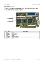
Page 27: ...interfaces allowing transfer rates of up to 3 Gbit per second These interfaces are made available via two 7 pin connectors The required settings are made in the BIOS setup Pinbelegung SATA Pin Name Beschreibung 1 GND Masse 2 SATATX SATA Senden 3 SATATX SATA Senden 4 GND Masse 5 SATARX SATA Empfangen 6 SATARX SATA Empfangen 7 GND Masse ...

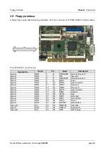
Page 28: ...bit 11 data bit 3 PDD3 11 12 PDD12 data bit 12 data bit 2 PDD2 13 14 PDD13 data bit 13 data bit 1 PDD1 15 16 PDD14 data bit 14 data bit 0 PDD0 17 18 PDD15 data bit 15 ground GND 19 20 N C coded DMA request signal PDDREQ 21 22 GND ground write signal PDIOW 23 24 GND ground read signal PDIOR 25 26 GND ground ready signal PDRDY 27 28 N C reserved DMA acknowledge signal PDDACK 29 30 GND ground interru...

Page 29: ...ground GND 3 4 N C reserved ground GND 5 6 DRVDEN1 drive density sel 1 ground GND 7 8 IDX index ground GND 9 10 MT0 motor enable 0 ground GND 11 12 DR1 drive sel 1 ground GND 13 14 DR0 drive sel 0 ground GND 15 16 MT1 motor enable 1 ground GND 17 18 DIR direction ground GND 19 20 STP step ground GND 21 22 WD write data ground GND 23 24 WE write enable ground GND 25 26 TR0 track 0 ground GND 27 28 ...

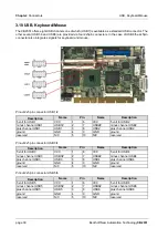
Page 30: ...el USB1 USB1 2 7 USB2 minus channel USB2 plus channel USB1 USB1 3 8 USB2 plus channel USB2 ground GND 4 9 GND ground reserved N C 5 10 N C reserved Pinout 2x5 pin connector USB 3 4 Description Name Pin Name Description 5 volt for USB3 VCC 1 6 VCC 5 volt for USB4 minus channel USB3 USB3 2 7 USB4 minus channel USB4 plus channel USB3 USB3 3 8 USB4 plus channel USB4 ground GND 4 9 GND ground reserved ...

Page 31: ...me Description 5 volt for USB8 VCC 1 6 VCC 5 volt supply minus channel USB8 USB8 2 7 KCLK keyboard clock plus channel USB8 USB8 3 8 KDAT keyboard data ground GND 4 9 MCLK mouse clock reserved N C 5 10 MDAT mouse data Pinout USB connector for channel X Pin Name Description 1 VCC 5 volt for USBX 2 USBX minus channel USBX 3 USBX plus channel USBX 4 GND ground ...

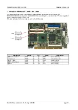
Page 32: ...LFSN mating connector PHDR 10VS According to the product order TTL level signals or RS232 standard signals are provided The port address and the interrupt are set via the BIOS setup Description Name Pin Name Description data carrier detect DCD 1 6 DSR data set ready receive data RXD 2 7 RTS request to send transmit data TXD 3 8 CTS clear to send data terminal ready DTR 4 9 RI ring indicator ground...

Page 33: ...LFSN mating connector PHDR 10VS According to the product order TTL level signals or RS232 standard signals are provided The port address and the interrupt are set via the BIOS setup Description Name Pin Name Description data carrier detect DCD 1 6 DSR data set ready receive data RXD 2 7 RTS request to send transmit data TXD 3 8 CTS clear to send data terminal ready DTR 4 9 RI ring indicator ground...

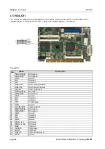
Page 34: ...VI data 2 3 GND ground 4 N C reserved 5 N C reserved 6 DDC CLK DDC clock DVI VGA 7 DDC DAT DDC data DVI VGA 8 VSYNC VGA vertical sync 9 TMDSDAT1 DVI data 1 10 TMDSDAT1 DVI data 1 11 GND ground 12 N C reserved 13 N C reserved 14 VCC 5 volt supply 15 GND ground 16 HP_DETECT hot plug detect 17 TMDSDAT0 DVI data 0 18 TMDSDAT0 DVI data 0 19 GND ground 20 N C reserved 21 N C reserved 22 GND ground 23 TM...

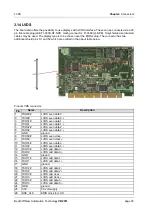
Page 35: ...low Pinout LVDS connector Pin Name Description 1 TXO00 LVDS even data 0 2 TXO00 LVDS even data 0 3 TXO01 LVDS even data 1 4 TXO01 LVDS even data 1 5 TXO02 LVDS even data 2 6 TXO02 LVDS even data 2 7 GND ground 8 TXO0C LVDS even clock 9 TXO0C LVDS even clock 10 TXO03 LVDS even data 3 11 TXO03 LVDS even data 3 12 TXO10 LVDS odd data 0 13 TXO10 LVDS odd data 0 14 GND ground 15 TXO11 LVDS odd data 1 1...

Page 36: ...nectors LVDS page 36 Beckhoff New Automation Technology CB2051 Pin Name Description 27 DDC_DAT EDID data for LCD 28 FP_3 3V switched 3 3 volt for display 29 FP_BL switched 5 volt for backlight 30 VCC 5 volt supply ...

Page 37: ...th automatic bandwidth selection It also offers auto cross and auto negotiate functionality The controller chip is the Intel 82562 PXE and RPL functions are also supported Pinout LAN 10 100 Pin Name Description 1 LAN1 0 LAN1 transmit plus 2 LAN1 0 LAN1 transmit minus 3 LAN1 1 LAN1 receive plus 4 N C reserved 5 N C reserved 6 LAN1 1 LAN1 receive minus 7 N C reserved 8 N C reserved ...

Page 38: ...r auto cross and auto negotiate functionality The controller chip is the Intel 82573L E PXE and RPL functions are not supported Pinout LAN 10 100 1000 Pin Name Description 1 LAN2 0 LAN2 channel 0 plus 2 LAN2 0 LAN2 channel 0 minus 3 LAN2 1 LAN2 channel 1 plus 4 LAN2 2 LAN2 channel 2 plus 5 LAN2 2 LAN2 channel 2 minus 6 LAN2 1 LAN2 channel 1 minus 7 LAN2 3 LAN2 channel 3 plus 8 LAN2 3 LAN2 channel ...

Page 39: ...ing jumper which if shorted at boot time triggers the NVRST signal in the controller thereby resetting all parameters of NVRAM to default values Conversion to the respective connector of the touch screen must be provided externally Please consult the manufacturer s documentation to figure out the relevant technical details Note In the pinout table below H X S Y and L are the signal names in the ca...

Page 40: ...ailable Signals SPDIFI and SPDIFO provide digital input and output If a transformation to a coaxial or optical connector is necessary this must be performed externally Pinout audio 2x5 pin connector Description Name Pin Name Description digital output SPDIF SPDIFO 1 6 3 3V 3 3 volt supply digital input SPDIF SPDIFI 2 7 S_AGND analog ground sound sound output right front output right LOUT_R FRONT_R...

Page 41: ...pport Description Name Pin Name Description 5 volt supply VCC 1 11 VCC 5 volt supply GP input output 10 GPIO10 2 12 GPIO20 GP input output 20 GP input output 11 GPIO11 3 13 GPIO21 GP input output 21 GP input output 12 GPIO12 4 14 GPIO22 GP input output 22 GP input output 13 GPIO13 5 15 GPIO23 GP input output 23 GP input output 14 GPIO14 6 16 GPIO24 GP input output 24 GP input output 15 GPIO15 7 17...

Page 42: ...rough a 2x5 pin connector JST B10B PHDSSLFSN mating connector PHDR 10VS The SMBus signals are processed by the chipset the I2C signals are processed by the SIO unit Pinout SMBus I2C connector Description Name Pin Name Description 3 3 volt supply 3 3V 1 6 GND ground SMBus clock SMBCLK 2 7 SMBDAT SMBus data SMBus alarm SMBALRT 3 8 SVCC standby supply 5V I2C bus clock I2CLK 4 9 I2DAT I2C bus data 5 v...

Page 43: ...1Fan Connectors Two 3 pin connectors are available for controlling and monitoring external fans 12 volt For the monitoring the fans must provide a corresponding speed signal Pinout fan connector Pin Name Description 1 GND ground 2 12V 12 volt supply regulated 3 TACHO fan monitoring signal ...

Page 44: ... pages are meant to be examples only They do not represent the recommended settings or the default settings Determination of the appropriate settings is dependent upon the particular application scenario in which the board is used 4 2 Top Level Menu Phoenix AwardBIOS CMOS Setup Utility Standard CMOS Features Frequency Voltage Control Advanced BIOS Features Load Fail Safe Defaults Advanced Chipset ...

Page 45: ...lue F10 Save ESC Exit F1 Help F5 Previous Values F6 Fail Safe Defaults F7 Optimized Defaults Date mm dd yy Options mm month dd day yy year Time hh mm ss Options hh hours mm minutes ss seconds IDE Channel 0 Master Sub menu see IDE Channel 0 Master Slave page 47 IDE Channel 0 Slave Sub menu see IDE Channel 0 Master Slave page 47 IDE Channel 1 Master Sub menu see IDE Channel 0 Master Slave page 47 ID...

Page 46: ... CMOS Features page 46 Beckhoff New Automation Technology CB2051 Halt On Options All Errors No Errors All But Keyboard All But Diskette All But Disk Key Base Memory Options none Extended Memory Options none Total Memory Options none ...

Page 47: ...uto Access Mode Auto Capacity 0 MB Cylinder 0 Head 0 Precomp 0 Landing Zone 0 Sector 0 Move Enter Select PU PD Value F10 Save ESC Exit F1 Help F5 Previous Values F6 Fail Safe Defaults F7 Optimized Defaults IDE HDD Auto Detection Options none IDE Channel 0 Master Options None Auto Manual Access Mode Options CHS LBA Large Auto Capacity Options none Cylinder Options none Head Options none Precomp Opt...

Page 48: ...cess Mode Auto Capacity 0 MB Cylinder 0 Head 0 Precomp 0 Landing Zone 0 Sector 0 Move Enter Select PU PD Value F10 Save ESC Exit F1 Help F5 Previous Values F6 Fail Safe Defaults F7 Optimized Defaults IDE Auto Detection Options none Extended IDE Drive Options None Auto Access Mode Options Large Auto Capacity Options none Cylinder Options none Head Options none Precomp Options none Landing Zone Opti...

Page 49: ... Version Control For OS 1 4 OS Select For DRAM 64MB Non OS2 HDD S M A R T Capability Enabled Full Screen LOGO Show Disabled Move Enter Select PU PD Value F10 Save ESC Exit F1 Help F5 Previous Values F6 Fail Safe Defaults F7 Optimized Defaults CPU Feature Sub menu see CPU Feature page 51 Hard Disk Boot Priority Sub menu see Hard Disk Boot Priority page 52 Virus Warning Options Enabled Disabled CPU ...

Page 50: ... Fast Typematic Rate Setting Options Enabled Disabled Typematic Rate Chars Sec Options 6 8 10 12 15 20 24 30 Typematic Delay Msec Options 250 500 750 1000 Security Option Options Setup System APIC Mode Options Enabled Disabled MPS Version Control For OS Options 1 1 1 4 OS Select For DRAM 64MB Options Non OS2 OS2 HDD S M A R T Capability Options Enabled Disabled Full Screen LOGO Show Options Enable...

Page 51: ...TM disable Item Help C1E Function Auto Execute Disable Bit Enabled Virtualization Technology Enabled Move Enter Select PU PD Value F10 Save ESC Exit F1 Help F5 Previous Values F6 Fail Safe Defaults F7 Optimized Defaults Delay Prior to Thermal Options none C1E Function Options Auto Disabled Execute Disable Bit Options Enabled Disabled Virtualization Technology Options Enabled Disabled ...

Page 52: ...PU PD Change Priority F10 Save ESC Exit F5 Previous Values F6 Fail Safe Defaults F7 Optimized Defaults list of available devices Options this dialog allows you to set the order in which the available bootable devices shall be accessed for an attempt to boot Attention in this sub menu the buttons Page Up Page Down and have a different function than in the rest of the setup They serve to move the it...

Page 53: ...D Memory Size 128MB Boot Display Auto Panel Scaling Auto Panel Number 640x480 Move Enter Select PU PD Value F10 Save ESC Exit F1 Help F5 Previous Values F6 Fail Safe Defaults F7 Optimized Defaults DRAM Timing Selectable Options By SPD Manual CAS Latency Time Options 5 4 3 6 Auto DRAM RAS to CAS Delay Options 2 3 4 5 6 Auto DRAM RAS Precharge Options 2 3 4 5 6 Auto Precharge delay tRAS Options Auto...

Page 54: ...Buffer Size Options 1MB 8MB DVMT Mode Options FIXED DVMT BOTH DVMT FIXED Memory Size Options 64MB 128MB 224MB Boot Display Options VBIOS Default LFP EFP EFP2 Panel Scaling Options Auto On Off Panel Number Options 640x480 800x600 1024x768 1280x1024 1400x1050 1600x1200 1280x768 1680x1050 1920x1200 1280x800 1440x900 ...

Page 55: ...s Port 2 Auto PCI Express Port 3 Auto PCI Express Port 4 Auto PCI E Compliancy Mode v1 0a Move Enter Select PU PD Value F10 Save ESC Exit F1 Help F5 Previous Values F6 Fail Safe Defaults F7 Optimized Defaults PCI Express Port 1 Options Auto Enabled Disabled PCI Express Port 2 Options Auto Enabled Disabled PCI Express Port 3 Options Auto Enabled Disabled PCI Express Port 4 Options Auto Enabled Disa...

Page 56: ...rals OnChip IDE Device Press Enter Item Help Onboard Device Press Enter SuperIO Device Press Enter Move Enter Select PU PD Value F10 Save ESC Exit F1 Help F5 Previous Values F6 Fail Safe Defaults F7 Optimized Defaults OnChip IDE Device Sub menu see OnChip IDE Devices page 57 Onboard Device Sub menu see Onboard Devices page 58 SuperIO Device Sub menu see SuperIO Devices page 59 ...

Page 57: ... is Primary Move Enter Select PU PD Value F10 Save ESC Exit F1 Help F5 Previous Values F6 Fail Safe Defaults F7 Optimized Defaults IDE HDD Block Mode Options Enabled Disabled IDE DMA transfer access Options Enabled Disabled On Chip Primary PCI IDE Options Enabled Disabled IDE Primary Master PIO Options Auto Mode 0 Mode 1 Mode 2 Mode 3 Mode 4 IDE Primary Slave PIO Options Auto Mode 0 Mode 1 Mode 2 ...

Page 58: ... Enabled USB Keyboard Support Disabled Azalia AC97 Audio Auto Touch Enabled Move Enter Select PU PD Value F10 Save ESC Exit F1 Help F5 Previous Values F6 Fail Safe Defaults F7 Optimized Defaults USB Controller Options Enabled Disabled USB 2 0 Controller Options Enabled Disabled USB Keyboard Support Options Enabled Disabled Azalia AC97 Audio Select Options Auto AC97 Audio only All Disabled Touch Op...

Page 59: ...ial Port 4 2E8 IRQ10 Move Enter Select PU PD Value F10 Save ESC Exit F1 Help F5 Previous Values F6 Fail Safe Defaults F7 Optimized Defaults Onboard FDC Controller Options Enabled Disabled Onboard Serial Port 1 Options Disabled 3F8 IRQ4 2F8 IRQ3 3E8 IRQ4 2E8 IRQ3 Auto Onboard Serial Port 2 Options Disabled 3F8 IRQ4 2F8 IRQ3 3E8 IRQ4 2E8 IRQ3 Auto UART Mode Select Options IrDA ASKIR Normal RxD TxD A...

Page 60: ...egrated Peripherals page 60 Beckhoff New Automation Technology CB2051 Onboard Serial Port 3 Options Disabled 3F8 IRQ11 2F8 IRQ11 3E8 IRQ11 2E8 IRQ11 Onboard Serial Port 4 Options Disabled 3F8 IRQ10 2F8 IRQ10 3E8 IRQ10 2E8 IRQ10 ...

Page 61: ...y Alarm Disabled x Date of Month Alarm 0 x Time hh mm ss 0 0 0 Move Enter Select PU PD Value F10 Save ESC Exit F1 Help F5 Previous Values F6 Fail Safe Defaults F7 Optimized Defaults ACPI function Options Enabled Disabled ACPI Suspend Type Options S1 POS S3 STR S1 S3 Run VGABIOS if S3 Resume Options Auto Yes No Power Management Options User Define Min Saving Max Saving Video Off Method Options Blan...

Page 62: ...e by Alarm Options Enabled Disabled Date of Month Alarm Options 1 31 Time hh mm ss Alarm Options insert hh mm and ss Primary IDE 0 Options Enabled Disabled Primary IDE 1 Options Enabled Disabled Secondary IDE 0 Options Enabled Disabled Secondary IDE 1 Options Enabled Disabled FDD COM LPT Port Options Enabled Disabled PCI PIRQ A D Options Enabled Disabled HPET Support Options Enabled Disabled HPET ...

Page 63: ...d PCI Express relative items Maximum Payload Size 128 Move Enter Select PU PD Value F10 Save ESC Exit F1 Help F5 Previous Values F6 Fail Safe Defaults F7 Optimized Defaults Init Display First Options PCI Slot Onboard Reset Configuration Data Options Enabled Disabled Resources Controlled By Options Auto ESCD Manual IRQ Resources Sub menu see IRQ Resources page 64 PCI VGA Palette Snoop Options Enabl...

Page 64: ...to PCI Device IRQ 15 assigned to PCI Device Move Enter Select PU PD Value F10 Save ESC Exit F1 Help F5 Previous Values F6 Fail Safe Defaults F7 Optimized Defaults IRQ 3 assigned to Options PCI Device Reserved IRQ 4 assigned to Options PCI Device Reserved IRQ 5 assigned to Options PCI Device Reserved IRQ 7 assigned to Options PCI Device Reserved IRQ 9 assigned to Options PCI Device Reserved IRQ 10 ...

Page 65: ...1 50V 5 V 12 V 4 92V 11 64V 12 V DDR VTT 12 31V 0 91V S3 3 V S1 2 V 3 31V 1 20V VBatt 3 28V Fan1 2 Speed 4166 RPM 0 RPM Board Revision 1 Move Enter Select PU PD Value F10 Save ESC Exit F1 Help F5 Previous Values F6 Fail Safe Defaults F7 Optimized Defaults On Die Digital Temp Options none Temp Board Options none Temp DDR Options none CPU Core Options none GMCH Core Options none CPU VTT Options none...

Page 66: ...Chapter BIOS Settings PC Health Status page 66 Beckhoff New Automation Technology CB2051 S3 3 V S1 2 V Options none VBatt Options none Fan1 2 Speed Options none Board Revision Options none ...

Page 67: ...BIOS CMOS Setup Utility Frequency Voltage Control Auto Detect PCI Clk Enabled Item Help Spread Spectrum 0 25 Move Enter Select PU PD Value F10 Save ESC Exit F1 Help F5 Previous Values F6 Fail Safe Defaults F7 Optimized Defaults Auto Detect PCI Clk Options Enabled Disabled Spread Spectrum Options Disabled 0 25 0 5 0 75 1 0 125 0 25 0 375 0 5 ...

Page 68: ... required parameters 4 12Load Optimized Defaults This option applies like described under Remarks for Setup Use 5 1 At first start of the BIOS optimized values are loaded from the setup which are supposed to make the board boot This status is achieved again if the board is reprogrammed using the flash program with the required parameters 4 13Set Password Here you can enter a password to protect th...

Page 69: ...ngly recommended This ensures that the new BIOS works correctly and that all chipset registers which were saved in the setup are reinitialized through the BIOS DMI should only be erased option cd if the BIOS supplier advises to do so A complete description of all valid parameters is shown with the parameter In order to make the updating process run automatically the parameter py must be added This...

Page 70: ...Chapter Mechanical Drawings PCB Mounting Holes page 70 Beckhoff New Automation Technology CB2051 6 Mechanical Drawings 6 1 PCB Mounting Holes NOTE All dimensions are in mil 1 mil 0 0254 mm ...

Page 71: ...PCB Pin1 Dimensions Chapter Mechanical Drawings Beckhoff New Automation Technology CB2051 page 71 6 2 PCB Pin1 Dimensions NOTE All dimensions are in mil 1 mil 0 0254 mm ...

Page 72: ...Chapter Mechanical Drawings PCB Die Center page 72 Beckhoff New Automation Technology CB2051 6 3 PCB Die Center NOTE All dimensions are in mil 1 mil 0 0254 mm ...

Page 73: ...1 0 C per minute Shipping 1 0 C per minute for packaged boards Relative Humidity Operating 5 up to 85 non condensing Storage 5 up to 95 non condensing Shipping 5 up to 100 non condensing for packaged boards Shock Operating 150m s 2 6ms Storage 400m s 2 6ms Shipping 400m s 2 6ms for packaged boards Vibration Operating 10 up to 58Hz 0 075mm amplitude 58 up to 500Hz 10m s 2 Storage 5 up to 9Hz 3 5mm ...

Page 74: ...fect the cooling concept The power consumption of such components may be comparable to the consumption of the processor The board design includes thermal solution mounting points that will provide the best possible thermal interface between die and solution Since we take thermal solutions seriously we have several advanced aggressive cooling solutions in our product portfolio Please contact your s...

Page 75: ...umentation for Beckhoff components there 8 2 Beckhoff Headquarters Beckhoff Automation GmbH Eiserstr 5 33415 Verl Germany phone 49 0 5246 963 0 fax 49 0 5246 963 198 e mail info beckhoff com web www beckhoff com 8 2 1 Beckhoff Support Support offers you comprehensive technical assistance helping you not only with the application of individual Beckhoff products but also with other wide ranging serv...

Page 76: ...Annex Post Codes page 76 Beckhoff New Automation Technology CB2051 ...

Page 77: ...re interrupts will point on SPURIOUS_INT_HDLR and the software interrupts will point on SPURIOUS_soft_HDLR 1Dh Initialise Variable Routine EARLY_PM_INIT 1Fh Load the keyboard table Notebooks 21h Initialising of the hardware power management HPM Notebooks 23h 1 Test the validity of the RTC values Example 5Ah is an invalid value for an RTC minute 2 Load the CMOS values into the BIOS Stack Default va...

Page 78: ...all INT 15h with AX Reg E820h 69h Enable level 2 cache 6Bh Programming of the chip set register according to the BIOS set up and auto detection table 6Dh 1 Assignment of resources for all ISA plug and play devices 2 Assignment of the port address for onboard COM ports only if an automatic junction has been defined in the setup 6Fh 1 Initialising of the floppy controller 2 Programming of all releva...

Page 79: ...ettings of keyboard LED and keyboard repeat rates 96h 1 Multi processor system generate MP table 2 Generate and update ESCD table 3 Correct century settings in the CMOS 20xx or 19xx 4 Synchronise the DOS system timer with CMOS time 5 Generate an MSIRQ Routing table C0h Chip set initialising Cut off shadow RAM Cut off L2 cache apron 7 or older Initialise chip set register C1h Memory detection Auto ...

Page 80: ...ge The used resources depend on setup settings If the entire range is clogged through option ROMs these functions do not work anymore Address Function A0000 BFFFF VGA RAM C0000 CFFFF VGA BIOS D0000 DFFFF AHCI BIOS RAID PXE if available E0000 EFFFF System BIOS while booting F0000 FFFFF System BIOS Interrupt The used resources depend on setup settings The listed interrupts and their use are given th...

Page 81: ... 2 USB UHCI Controller 3 ICH ID27CA 13 D 0 29 3 USB UHCI Controller 4 ICH ID27CB 13 A 0 29 7 USB 2 0 EHCI Controller ICH ID27CC 14 0 30 0 PCI to PCI Bridge ICH ID244E 14 A 0 30 2 AC 97 Audio Controller ICH ID27DE 14 B 0 30 3 AC 97 Modem Controller ICH 15 0 31 0 LPC Controller ICH ID27B8 15 A 0 31 1 IDE Controller ICH ID27DF 15 B 0 31 2 SATA Controller ICH 15 B 0 31 3 SMBus Controller ICH ID27DA 19...

Page 82: ...Annex Resources page 82 Beckhoff New Automation Technology CB2051 Address Function A2 A3 DIMM 2 A4 AF BIOS internal B0 BF BIOS internal D2 D3 Clock ...

Reviews: