ADVANCE INFORMATION
VCT 49xxI
Volume 1: General Description
Pin Descriptions
Supply Pins
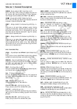
VSUP1.8DIG
−
Supply Voltage 1.8 V
This pin is main and standby supply for the digital core
logic of controller, video, display and deflection pro-
cessing.
VSUP1.8FE
−
Supply Voltage 1.8 V
This pin is main supply for the analog video front-end.
VSUP3.3FE
−
Supply Voltage 3.3 V
This pin is main supply for the analog video front-end.
VSUP3.3IO
−
Supply Voltage 3.3 V
This pin is main and standby supply for the digital I/O-
ports.
VSUP3.3DIG
−
Supply Voltage 3.3 V
This pin is main supply for the digital core logic of IF
and audio processing and digital video back-end.
VSUP3.3BE
−
Supply Voltage 3.3 V
This pin is main supply for the analog video back-end.
VSUP5.0BE
−
Supply Voltage 5.0 V
This pin is main supply for the analog video back-end.
VSUP8.0AU
−
Supply Voltage 8.0 V
This pin is main supply for the analog audio process-
ing.
GND
−
Ground Platform
This pin is main ground for all above supplies.
VSUP3.3DAC
−
Supply Voltage 3.3 V
This pin is main supply for the video DACs.
GNDDAC
−
Ground for 3.3 V Video DAC Supply
VSUP5.0IF
−
Supply Voltage 5.0 V
This pin is main supply for the analog IF front-end.
GNDIF
−
Ground for 5.0 V IF Supply
VSUP3.3EIO
−
Supply Voltage 3.3 V
This pin is main and standby supply for the extended
digital I/O-ports available in QFP package only. It is
internally connected to
VSUP3.3IO.
GNDEIO
−
Ground for 3.3 V Extended I/O Supply
It is internally connected to GND.
Application Note:
All
GND
pins must be connected to a low-resistive
ground plane underneath the IC. All supply pins must
be connected separately with short and low-resistive
lines to the power supply. Decoupling capacitors from
VSUPxx
to
GND
have to be placed as closely as pos-
sible to these pins. It is recommended to use more
than one capacitor. By choosing different values, the
frequency range of active decoupling can be extended.
IF Pins
VREFIF
−
Reference Voltage for Analog IF (Fig. 4–9)
This pin must be connected to
GNDIF
via a circuitry
according to the application circuit. Low inductance
caps are necessary.
IFIN+, IFIN-
−
Balanced IF Input (Fig. 4–6)
These pins must be connected to the SAW filter out-
put. The SAW filter has to be placed as close as possi-
ble. The layout of the IF input should be symmetrical
with respect to
GNDIF
.
SIF
−
2nd Sound IF Output (Fig. 4–8)
Output level is set via I
2
C-Bus. An appropriate sound
processor (e.g. MSP) can be connected to this pin.
This pin is also configurable as audio input (see
Fig. 4–10).
TAGC
−
Tuner AGC Output (Fig. 4–7)
This pin controls the delayed tuner AGC. As it is a
noise-shaped-I-DAC output, it has to be connected
according to the application circuit.
Audio Pins
VREFAU
– Reference Voltage for Analog Audio (Fig.
4–14)
This pin serves as the internal ground connection for
the analog audio circuitry. It must be connected to the
GND
pin with a 3.3
µ
F and a 100 nF capacitor in paral-
lel. This pins shows a DC level of typically 3.77 V.
AIN1 L
– Audio 1 Inputs (Fig. 4–10)
The analog input signal for audio 1 is fed to this pin.
Analog input connection must be AC coupled.
AIN1 R
– Audio 1 Inputs (Fig. 4–10)
The analog input signal for audio 1 is fed to this pin.
Analog input connection must be AC coupled. This pin
is also configurable as sound IF output (see Fig. 4–8).
AIN2 R/L
– Audio 2 Inputs (Fig. 4–10)
The analog input signal for audio 2 is fed to this pin.
Analog input connection must be AC coupled.
AIN3 R/L
– Audio 3 Inputs (Fig. 4–10)
The analog input signal for audio 3 is fed to this pin.
Analog input connection must be AC coupled.


