ADVANCE INFORMATION
VCT 49xxI
Volume 1: General Description
SENSE
−
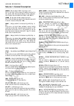
Measurement ADC Input (Fig. 4–27)
This is the input of the analog to digital converter for
the picture and tube measurement. Three measure-
ment ranges are selectable with RSW1 and RSW2.
GNDM
−
Measurement ADC Reference Input
This is the reference ground for the measurement A/D
converter. Connect this pin to GND.
RSW1
−
Range Switch1 for Measuring ADC (Fig. 4–
25)
These pin is an open drain pulldown output. During
cutoff and white drive measurement the switch is off.
During the rest of time it is on. The RSW1 pin can be
used as second measurement ADC input for picture
beam current measurement.
RSW2
−
Range Switch2 for Measuring ADC (Fig. 4–
26)
These pin is an open drain pulldown output. During
cutoff measurement the switch is off. During white
drive measurement the switch is on. Also during the
rest of time it is on. It is used to set the range for white
drive current measurement.
4.3.6. Controller Pins
XTAL1
−
Crystal Input and
XTAL2
Crystal Output (Fig.
4–28)
These pins connect a 20.25 MHz crystal to the internal
oscillator. An external clock can be fed into XTAL1.
RESETQ
−
Reset Input/Output (Fig. 4–29)
A low level on this pin resets the VCT 49xxI. The inter-
nal CPU can pull down this pin to reset external
devices connected to this pin.
TEST
−
Test Input (Fig. 4–30)
This pin enables factory test modes. For normal opera-
tion, it must be connected to ground.
SCL
−
I
2
C Bus Clock (Fig. 4–31)
This pin delivers the I
2
C bus clock line. The signal can
be pulled down by external slave ICs to slow down
data transfer.
SDA
−
I
2
C Bus Data (Fig. 4–31)
This pin delivers the I
2
C bus data line.
P10
−
P13, P20
−
P23
−
I/O Port (Fig. 4–32)
These pins provide CPU controlled I/O ports.
P14
−
P17
−
I/O Port (Fig. 4–33)
These pins provide CPU controlled I/O ports. Addition-
ally they can be used as analog inputs for the control-
ler ADC.
P24
−
P26, P30
−
P37
−
I/O Port (Fig. 4–34)
These pins provide CPU controlled I/O ports.
ADB0
−
ADB19
−
Address Bus Output (Fig. 4–35)
These 20 lines provide the CPU address bus output to
access external memory.
DB0
−
DB7
−
Data Bus Input/Output (Fig. 4–36)
These 8 lines provide the bidirectional CPU data bus
to access external memory.
WRQ
−
Data Write Enable Output (Fig. 4–35)
This pin controls the direction of data exchange
between the CPU and the external data memory
device (SRAM).
RDQ
−
Data Read Enable Output (Fig. 4–35)
This pin is used to enable the output driver of the
external data memory device (SRAM) for read access.
PSENQ
−
Program Store Enable Output (Fig. 4–35)
This pin is used to enable the output driver of the
external program memory device (ROM/FLASH) for
read access.
PSWEQ
−
Program Store Write Enable Output (Fig. 4–
35)
This pin is used to write into the external program flash
memory device.
XROMQ
−
External ROM Enable Input (Fig. 4–37)
This pin must be pulled low to access the external pro-
gram memory.
XROMQ
has an internal pull-up resis-
tor.
EXTIFQ
−
Enable External Memory Interface Input
(Fig. 4–37)
This pin must be pulled low to enable the external
memory interface.
EXTIFQ
has an internal pull-up
resistor.
STOPQ
−
Stop CPU Input (Fig. 4–37)
Applying a low level during the input phase freezes the
realtime relevant internal peripherals such as timers
and interrupt controller.
STOPQ
has an internal pull-up
resistor.
ENEQ
−
Enable Emulation Input (Fig. 4–37)
Only if this pin is set to low level, STOPQ and OCF are
operational.
ENEQ
has an internal pull-up resistor.
ALE
−
Address Latch Enable Output (Fig. 4–35)
This signal indicates changes on the address bus.
OCF
−
Opcode Fetch Output (Fig. 4–35)
A high level driven by the CPU during output phase
indicates the beginning of a new instruction.
RSTQ
−
Internal CPU Reset Input/Output (Fig. 4–38)
This pin is used for emulation purpose only. A low level
on this pin resets the CPU. It also indicates an internal
reset of the CPU.


