27.1.1999
8dds50gb_fm5.fm
7
Product: DDS-50(Office set) / YO0311
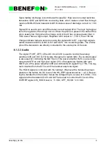
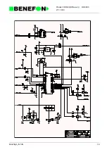
8.1.3 Operation
8.1.3.1 General
Power supply unit is connected to one of the connectors on the back of the unit.
Connections on these two connectors are identical to each other. Supply voltage
(VB) turns on regulator I124 which is used to ge5 VDC supply (VCC) for pro-
cessor and other electronics. Note that the power amplifiers of the earphone signal,
I499 and I528 do not use VCC but VB instead. Once the VCC signal has risen, also
signal CADET is activated. This causes the phone to communicate with the I2C cir-
cuit and register that office kit is present.
8.1.3.2 Processor / charging
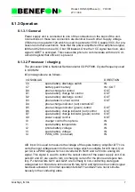
The processor I264 is National Semiconductor COPCF888. Crystal frequency used
is 8,00 MHz.
I/O pins/signals are as follows:
A/D input I3 is used to measure the voltage of the spare battery. Amplifier I277 con-
verts the input voltage level into the new range which is suitable for A/D input. Out-
put G3 is a PWM signal which is converted with R291 and C293 into analog DC
signal. This signal is used to control the output current of the power supply unit. Out-
puts D0 and D1 are used to turn on charging current for the phone and spare bat-
tery. P-channel fets Q211 and Q221 are normally in non-conducting state (gate
voltage tied to VB) and are turned on with fets Q212 and Q222 as the control signal
has been activated. In normal operation fets Q211 and Q221 are never simulta-
neously in the conducting state.
I/O SIGNALS
DIRECTION
C0
spare battery discharge switch
IN
C7
battery pack memory
IN / OUT
D0
phone charge fet control
OUT
D1
spare battery charge fet control
OUT
D2
spare battery discharge control
OUT
D3
phone detect current control
OUT
D4
phone charge indicator (red) controlOUT
D5
phone charge indicator (green) control
OUT
D6
spare battery charge indicator (red) control
OUT
D7
spare battery charge indicator (green) control
OUT
G3
power supply control
OUT
I0
charger control from phone
IN
I1
spare battery temperature
IN
I2
phone battery voltage
IN
I3
spare battery voltage
IN
I4
PWM_CHK (not used)
IN
Summary of Contents for SIGMA GOLD TDP-52-SN3
Page 1: ...27 1 1999 Dp_52ngbTOC fm 1 Product TDP 52 SN3 SERVICE MANUAL BENEFON SIGMA GOLD TDP 52 SN3 ...
Page 12: ...27 1 1999 2DP_52GB 7 Product TDP 52 SN3 General Line interface Branching unit LIF 40 DB 40 ...
Page 15: ...1user_gb fm 1 2 0 OWNER S MANUAL ...
Page 57: ...27 1 1999 4A0701GB __1 23 Product TDP 52 SN3 Sigma Gold OA0701 Proc ...
Page 58: ...27 1 1999 4A0701GB __1 24 Product TDP 52 SN3 Sigma Gold OA0701 Proc ...
Page 59: ...27 1 1999 4A0701GB __1 25 Product TDP 52 SN3 Sigma Gold OA0701 Proc ...
Page 60: ...27 1 1999 4A0701GB __1 26 Product TDP 52 SN3 Sigma Gold OA0701 Proc ...
Page 61: ...27 1 1999 4A0701GB __1 27 Product TDP 52 SN3 Sigma Gold OA0701 Proc ...
Page 62: ...27 1 1999 4A0701GB __1 28 Product TDP 52 SN3 Sigma Gold OA0701 Proc ...
Page 67: ...27 1 1999 4H0700GB __2 33 Product TDP 52 SN3 Sigma Gold OH0700 The Top Side Layout PH0700 A5 ...
Page 69: ...27 1 1999 4H0700GB __2 35 Product TDP 52 SN3 Sigma Gold OH0700 ...
Page 84: ...27 1 1999 4Y0725GB 50 Product TDP 52 SN3 Sigma Gold OY0725 RF ...
Page 85: ...27 1 1999 4Y0725GB 51 Product TDP 52 SN3 Sigma Gold OY0725 RF ...
Page 86: ...27 1 1999 4Y0725GB 52 Product TDP 52 SN3 Sigma Gold OY0725 RF ...
Page 87: ...26 1 1999 8HAR_GB fm 1 6 0 CHARGING CHARGING ...
Page 90: ...26 1 1999 8CARA_GB fm 1 7 0 CAR ASSEMBLY KIT CAR ASSEMBLY KIT ...
Page 98: ...27 1 1999 8udh50gb_fm5 fm 9 Product UDH 50 Carbox OO0700 The Top Side Layout PW0700B2 ...
Page 99: ...27 1 1999 8udh50gb_fm5 fm 10 Product UDH 50 Carbox OO0700 The Bottom Side Layout PW0700B2 ...
Page 100: ...27 1 1999 8udh50gb_fm5 fm 11 Product UDH 50 Carbox OO0700 A2 ...
Page 101: ...27 1 1999 8udh50gb_fm5 fm 12 Product UDH 50 Carbox OO0700 A2 ...
Page 102: ...27 1 1999 8udh50gb_fm5 fm 13 Product UDH 50 Carbox OO0700 A2 ...
Page 103: ...27 1 1999 8udh50gb_fm5 fm 14 Product UDH 50 Carbox OO0700 A2 ...
Page 113: ...27 1 1999 8UDH50GB __1_f 24 Product UDH 50 Carbox OW0700 The Top Side Layout PW0700A5 ...
Page 114: ...27 1 1999 8UDH50GB __1_f 25 Product UDH 50 Carbox OW0700 The Bottom Side Layout PW0700A5 ...
Page 115: ...27 1 1999 8UDH50GB __1_f 26 Product UDH 50 Carbox OW0700 A5 ...
Page 116: ...27 1 1999 8UDH50GB __1_f 27 Product UDH 50 Carbox OW0700 A5 ...
Page 117: ...27 1 1999 8UDH50GB __1_f 28 Product UDH 50 Carbox OW0700 A5 ...
Page 118: ...27 1 1999 8UDH50GB __1_f 29 Product UDH 50 Carbox OW0700 A5 ...
Page 119: ...27 1 1999 8UDH50GB __1_f 30 Product UDH 50 Carbox OW0700 A5 ...
Page 124: ...27 1 1999 8kds50gb_fm5 fm 35 Product KDS 50 Hands free Cradle YO0701 KDS 50 ...
Page 131: ...27 1 1999 8HDS50GB_fm5 f 42 Product HDS 50 Ext Handset With Cradle HLS 41 HDS 50 HXS 40 ...
Page 133: ...27 1 1999 8OSET_GB fm 1 8 0 OFFICE SET OFFICE SET ...
Page 147: ...27 1 1999 8dds50gb_fm5 fm 15 Product DDS 50 Office set OO0303 ...
Page 148: ...27 1 1999 8dds50gb_fm5 fm 16 Product DDS 50 Office set OO0303 ...
Page 149: ...27 1 1999 8dds50gb_fm5 fm 17 Product DDS 50 Office set OO0303 ...
Page 151: ...27 1 1999 8dds50gb_fm5 fm 19 Product DDS 50 Office set OO0301 ...
Page 153: ...27 1 1999 8dds50gb_fm5 fm 21 Product DDS 50 Office set OO0302 ...
Page 154: ...27 1 1999 8dds50gb_fm5 fm 22 Product DDS 50 Office set OO0302 ...
Page 161: ...27 1 1999 8hxs40gb_fm5 fm 29 Product HXS 40 External Handset HLS 41 HDS 50 HXS 40 ...
Page 162: ...27 1 1999 8OTHE_GB fm 1 9 0 OTHER ACCESSORIES OTHER ACCESSORIES ...
Page 174: ...27 1 1999 Xo0245e4_fm5 fm 13 Product LIF 40 Line Interface OO0245 Solder Side Layout PO0245A0 ...
Page 175: ...27 1 1999 Xo0245e4_fm5 fm 14 Product LIF 40 Line Interface OO0245 ...
Page 176: ...27 1 1999 Xo0245e4_fm5 fm 15 Product LIF 40 Line Interface OO0245 ...
Page 177: ...27 1 1999 Xo0236e4_fm5 fm 16 Product DB 40 Branching Unit YO0236 9 2 BRANCHING UNIT YO0236 ...
Page 183: ...27 1 1999 Xo0236e4_fm5 fm 22 Product DB 40 Branching Unit OO0241 ...

