27.1.1999
4A0701GB.__1
11
Product: TDP-52-SN3 (Sigma Gold) / OA0700 Audio
transmit signal. VR3 is a maximum deviation gain control circuit to set the
transmit signal level. After the VR3 comes switch TXAUDON, which mutes the
tx-audio signal using the TXMUTE control. From the switch, the signal is fed to
the summing junction (ADD3) of the tx-audio signal, FFSK signal and Fii-
signal. Next comes VR4 gain control circuit to set. SMF1 is smoothing filter for
tx-audio signal. The tx-audio signal is then fed to the V102 connector pin 20.
5.1.7 RX-Audio
The rx-audio signal coming from the receiver through the V102 pin 8 is fed to
the audio circuit I405 pin 23. Inside the circuit, the signal is fed to the
operational amplifier (AMP2) inverting input. The amplifier gain is set by
resistors R440 and R441. The signal is next passed through an anti-aliasign
filter. VR5 is a gain control circuit to set the rx-audio signal to the correct level.
Next comes de-emphasis (D/E) circuit. Equalize the pre-empassized rx-audio
signal. The signal passes from the D/E through the switch RXAUDON. RXBPF
is the band-pass filter for the rx-audio signal. RXDET is the rx-audio signal
detection circuit. This circuit works as a full wave rectifier. After the RXBPF
comes expander circuit (EXP). Expand the rx-audio signal amplitude. It can be
bypassed. The linearity is adjustable by the control register EVR. VR6 is a gain
control circuit to set the rx-audio signal to the correct level. After VR6 comes
the RXMUTE switch, which is operated by the RXMUTE control. ADD4 is the
summing junction of the rx-audio signal, external signal (not used), DTMF
signal and transmit signal. VR10 is the volume control circuit to set the level of
earphone and external earphones. The rx-audio signal is connected through
the receiver driver (RECAMP) to the earphone.
5.1.8 FII Signal
The NMT system uses the FII signal to check the radio path quality. This
approx. 4kHz signal is split from the rx-audio signal after the VR5 and is filtered
through the band-pass filter (FBPF). VR7 sets the FII signal to the correct level.
Switch FILOOPON can be operated by the FIION control, to be summed with
the tx-audio signal before the VR4.
5.1.9 FFSK Modem
The FFSK data signal from FFSK modulator to be transmitted is passed
through the FFSK low-pass filter and pre-emphasis (FFSKP-EM) to the VR9,
which adjusts its level. The data signal is switched using switch FFSKTXON.
The data signal is summed with the tx-audio signal by the ADD3.
The received data signal is split from the rx-audio signal after the de-emphasis
circuit. The data signal is fed through the FFSK band-pass filter to the FFSK
demodulator and FFSK data detector.
FFSK DET block. The block works to judge the FFSK signal existence by
comparing the amplitude of the noise reduced FFSK signal and the provided
Summary of Contents for SIGMA GOLD TDP-52-SN3
Page 1: ...27 1 1999 Dp_52ngbTOC fm 1 Product TDP 52 SN3 SERVICE MANUAL BENEFON SIGMA GOLD TDP 52 SN3 ...
Page 12: ...27 1 1999 2DP_52GB 7 Product TDP 52 SN3 General Line interface Branching unit LIF 40 DB 40 ...
Page 15: ...1user_gb fm 1 2 0 OWNER S MANUAL ...
Page 57: ...27 1 1999 4A0701GB __1 23 Product TDP 52 SN3 Sigma Gold OA0701 Proc ...
Page 58: ...27 1 1999 4A0701GB __1 24 Product TDP 52 SN3 Sigma Gold OA0701 Proc ...
Page 59: ...27 1 1999 4A0701GB __1 25 Product TDP 52 SN3 Sigma Gold OA0701 Proc ...
Page 60: ...27 1 1999 4A0701GB __1 26 Product TDP 52 SN3 Sigma Gold OA0701 Proc ...
Page 61: ...27 1 1999 4A0701GB __1 27 Product TDP 52 SN3 Sigma Gold OA0701 Proc ...
Page 62: ...27 1 1999 4A0701GB __1 28 Product TDP 52 SN3 Sigma Gold OA0701 Proc ...
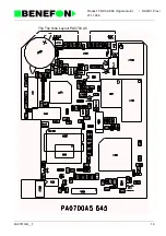
Page 67: ...27 1 1999 4H0700GB __2 33 Product TDP 52 SN3 Sigma Gold OH0700 The Top Side Layout PH0700 A5 ...
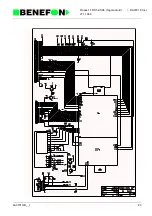
Page 69: ...27 1 1999 4H0700GB __2 35 Product TDP 52 SN3 Sigma Gold OH0700 ...
Page 84: ...27 1 1999 4Y0725GB 50 Product TDP 52 SN3 Sigma Gold OY0725 RF ...
Page 85: ...27 1 1999 4Y0725GB 51 Product TDP 52 SN3 Sigma Gold OY0725 RF ...
Page 86: ...27 1 1999 4Y0725GB 52 Product TDP 52 SN3 Sigma Gold OY0725 RF ...
Page 87: ...26 1 1999 8HAR_GB fm 1 6 0 CHARGING CHARGING ...
Page 90: ...26 1 1999 8CARA_GB fm 1 7 0 CAR ASSEMBLY KIT CAR ASSEMBLY KIT ...
Page 98: ...27 1 1999 8udh50gb_fm5 fm 9 Product UDH 50 Carbox OO0700 The Top Side Layout PW0700B2 ...
Page 99: ...27 1 1999 8udh50gb_fm5 fm 10 Product UDH 50 Carbox OO0700 The Bottom Side Layout PW0700B2 ...
Page 100: ...27 1 1999 8udh50gb_fm5 fm 11 Product UDH 50 Carbox OO0700 A2 ...
Page 101: ...27 1 1999 8udh50gb_fm5 fm 12 Product UDH 50 Carbox OO0700 A2 ...
Page 102: ...27 1 1999 8udh50gb_fm5 fm 13 Product UDH 50 Carbox OO0700 A2 ...
Page 103: ...27 1 1999 8udh50gb_fm5 fm 14 Product UDH 50 Carbox OO0700 A2 ...
Page 113: ...27 1 1999 8UDH50GB __1_f 24 Product UDH 50 Carbox OW0700 The Top Side Layout PW0700A5 ...
Page 114: ...27 1 1999 8UDH50GB __1_f 25 Product UDH 50 Carbox OW0700 The Bottom Side Layout PW0700A5 ...
Page 115: ...27 1 1999 8UDH50GB __1_f 26 Product UDH 50 Carbox OW0700 A5 ...
Page 116: ...27 1 1999 8UDH50GB __1_f 27 Product UDH 50 Carbox OW0700 A5 ...
Page 117: ...27 1 1999 8UDH50GB __1_f 28 Product UDH 50 Carbox OW0700 A5 ...
Page 118: ...27 1 1999 8UDH50GB __1_f 29 Product UDH 50 Carbox OW0700 A5 ...
Page 119: ...27 1 1999 8UDH50GB __1_f 30 Product UDH 50 Carbox OW0700 A5 ...
Page 124: ...27 1 1999 8kds50gb_fm5 fm 35 Product KDS 50 Hands free Cradle YO0701 KDS 50 ...
Page 131: ...27 1 1999 8HDS50GB_fm5 f 42 Product HDS 50 Ext Handset With Cradle HLS 41 HDS 50 HXS 40 ...
Page 133: ...27 1 1999 8OSET_GB fm 1 8 0 OFFICE SET OFFICE SET ...
Page 147: ...27 1 1999 8dds50gb_fm5 fm 15 Product DDS 50 Office set OO0303 ...
Page 148: ...27 1 1999 8dds50gb_fm5 fm 16 Product DDS 50 Office set OO0303 ...
Page 149: ...27 1 1999 8dds50gb_fm5 fm 17 Product DDS 50 Office set OO0303 ...
Page 151: ...27 1 1999 8dds50gb_fm5 fm 19 Product DDS 50 Office set OO0301 ...
Page 153: ...27 1 1999 8dds50gb_fm5 fm 21 Product DDS 50 Office set OO0302 ...
Page 154: ...27 1 1999 8dds50gb_fm5 fm 22 Product DDS 50 Office set OO0302 ...
Page 161: ...27 1 1999 8hxs40gb_fm5 fm 29 Product HXS 40 External Handset HLS 41 HDS 50 HXS 40 ...
Page 162: ...27 1 1999 8OTHE_GB fm 1 9 0 OTHER ACCESSORIES OTHER ACCESSORIES ...
Page 174: ...27 1 1999 Xo0245e4_fm5 fm 13 Product LIF 40 Line Interface OO0245 Solder Side Layout PO0245A0 ...
Page 175: ...27 1 1999 Xo0245e4_fm5 fm 14 Product LIF 40 Line Interface OO0245 ...
Page 176: ...27 1 1999 Xo0245e4_fm5 fm 15 Product LIF 40 Line Interface OO0245 ...
Page 177: ...27 1 1999 Xo0236e4_fm5 fm 16 Product DB 40 Branching Unit YO0236 9 2 BRANCHING UNIT YO0236 ...
Page 183: ...27 1 1999 Xo0236e4_fm5 fm 22 Product DB 40 Branching Unit OO0241 ...

