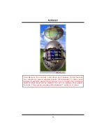
background image

M

M

M

7

7

7

V

V

V

I

I

I

Z

Z

Z

4

4

4

0

0

0

0

0

0


25


06/04/2004 

Summary of Contents for M7IZ400

Page 1: ...ference will not occur in a particular installation The vendor makes no representations or warranties with respect to the contents here of and specially disclaims any implied warranties of merchantability or fitness for any purpose Further the vendor reserves the right to revise this publication and to make changes to the contents here of without obligation to notify any party beforehand Duplicati...

Page 2: ...2 ENGLISH 3 M7VIZ400 Features 3 Package contents 4 How to set up Jumper 5 CPU Installation 5 DDR DIMM Modules DDR1 DDR2 6 Installing DDR Module 6 Jumpers Headers Connectors Slots 6 TROUBLESHOOTING 13 FRANÇAIS 14 Caractéristiques de la M7VIZ400 14 Contenu du carton 15 DÉPANNAGE 16 ii ...

Page 3: ...M M M7 7 7V V VI IIZ Z Z4 4 40 0 00 0 0 Layout of M7VIZ400 NOTE represents the first pin 1 ...

Page 4: ...or JPANEL1 F COM2 Header JCOM2 U Audio DJ Header JDJ1 G Game Port Header JGAME1 V System FAN Header JSFAN1 H Case Open Connector JCI1 W Serial ATA Connector JSATA1 2 I Power Source Selection for USB JUSBV1 X Front USB Header JUSB1 J Front 1394 Header J1394B1 Y Front USB Header JUSB2 K Accelerated Graphics Port Slot AGP1 Z Power Source Selection for USB JUSBV2 L PCI BUS Slots PCI 1 3 a1 Clear CMOS ...

Page 5: ...ec 1 0 Integrate Hardware Monitor functions Support Device Power Management DPM and ACPI Slots Three 32 bit PCI bus master slots One CNR slot only Type B One AGP 8X slot On Board IDE Supports four IDE disk drives Supports PIO Mode 4 Master Mode and Ultra DMA 33 66 100 133 Bus Master Mode LAN PHY Chip VIA VT6103 Supports 10 Mb s and 100 Mb s auto negotiation Half Full duplex capability IEEE 1394 Ch...

Page 6: ... audio header 1 S PDIF out header 1 1394A Firewire ports optional Dimensions ATX Form Factor 22 4cm X 24 3cm W X L B BIOS Software BIOS Award legal BIOS Supports APM1 2 Supports ACPI Supports USB Function Software Supports Warpspeeder 9th Touch and FLASHER Offers the highest performance for Windows 98 SE Windows 2000 Windows Me Windows XP UNIX and Linux Red Hat etc Package contents HDD Cable X 1 F...

Page 7: ...stallation Step1 Pull the lever sideways away from the socket and then raise the lever up to a 90 degree angle Step2 Look for the white dot cut edge The white dot cut edge should point wards the lever pivot The CPU will fit only in the correct orientation Step3 Hold the CPU down firmly and then close the lever to complete the installation Step4 Put the CPU Fan on the CPU and buckle it Connect the ...

Page 8: ...hip snap back in place and the DIMM is properly seated Jumpers Headers Connectors Slots Floppy Disk Connector FDD1 The motherboard provides a standard floppy disk connector that supports 360K 720K 1 2M 1 44M and 2 88M floppy disk types This connector supports the provided floppy drive ribbon cables Hard Disk Connectors IDE1 IDE2 The motherboard has a 32 bit Enhanced PCI IDE Controller that provide...

Page 9: ...has a PCI to SATA Controller with 2 channels SATA interface it satisfies the SATA 1 0 spec and can transfer data with 1 5 Gb s speed Note 1 When plugging SATA HDD on JSATA1 connector SATA BIOS will automatically detect as channel 1 2 When plugging SATA HDD on JSATA2 connector SATA BIOS will automatically detect as channel 0 Front Panel Connector JPANEL1 SPK PWR_LED HLED SLP RST 2 24 IR 1 23 IR ON ...

Page 10: ...the system via keyboard and mouse function JKBV1 jumper cap should be placed on pin 2 3 Power Source Selection for USB JUSBV1 JUSBV2 JUSBV3 JUSBV1 JUSBV2 JUSBV3 Assignment Description 1 3 Pin 1 2 close 5V JUSBV3 5V for USB located at the J1394_USB1 port connector JUSBV2 5V for USB located at the JUSB2 JUSB1 port connectors JUSBV1 5V for USB located at the JUSBLAN1 port connector 1 3 Pin 2 3 close ...

Page 11: ...five seconds 4 Set the jumper to Pin 1 2 Close 5 Power on the AC 6 Reset your desired password or clear the CMOS data Case Open Connector JCI1 Pin Assignment 1 Case Open Signal 1 JCI1 2 Ground Serial ATA Connector JSATA1 JSATA2 Pin Assignment Pin Assignment 1 Ground 2 TX 3 TX 4 Ground 5 RX 6 RX 1 2 3 4 5 6 7 JSATA1 JSATA2 7 Ground CD ROM Audio In Header JCDIN1 Pin Assignment 1 Left Channel Input 2...

Page 12: ...r Right 12 Right Line In Rear Speaker Right 13 Left Line In Rear Speaker Left 14 Left Line In Rear Speaker Left Digital Audio Connector JSPDIF1 Pin Assignment 1 5V 2 SPDIF_OUT 1 3 JSPDIF1 3 Ground Front USB Header JUSB2 JUSB1 Pin Assignment Pin Assignment 1 5V fused 2 5V fused 3 USB 4 USB 5 USB 6 USB 7 Ground 8 Ground 2 1 10 9 JUSB1 JUSB2 9 KEY 10 NC Front 1394 Header J1394B1 Pin Assignment Pin As...

Page 13: ...lection JCLK1 Pin 200 MHz 266 MHz Default 333 MHz 1 2 Close Open Open 3 4 Close Close Open 5 6 Open Open Open 7 8 Open Open Open Note Factory default setting is 266MHz Audio DJ JDJ1 Pin Assignment Pin Assignment 1 SMBDT 2 SMBCK 3 INTR_B 4 NA 1 5 JDJ1 5 PWRGD COM2 Header JCOM2 10 9 2 1 JCOM2 Pin Assignment Pin Assignment 1 RIN1 2 RIN3 3 DOUT2 4 DOUT3 5 Ground 6 RIN2 7 DOUT1 8 RIN4 9 XRI1 10 NA 11 ...

Page 14: ...ssignment 1 5V 2 5V 3 Joystick B Button 1 4 Joystick A Button 1 5 Joystick B Coordinate X 6 Joystick A Coordinate X 7 MIDI Output 8 Ground 9 Joystick B Coordinate Y 10 Ground 11 Joystick B Button 2 12 Joystick A Coordinate Y 13 MIDI Input 14 Joystick A Button 2 15 NA 16 5V Back Panel Connectors 12 ...

Page 15: ...from disk to disk controller board Make sure both ends are securely plugged in check the drive type in the standard CMOS setup Backing up the hard drive is extremely important All hard disks are capable of breaking down at any time System only boots from CD ROM Hard disk can be read and applications can be used but booting from hard disk is impossible Back up data and applications files Reformat t...

Page 16: ...cements PCI 32 bits bus maître Un emplacement CNR Type B uniquement Un emplacement AGP 8X IDE intégré Prend en charge quatre lecteurs de disques IDE Prend en charge les modes PIO 4 Maître et bus maître Ultra DMA 33 66 100 133 Réseau Puce VIA VT6103 Prend en charge la négociation automatique 10 Mb s et 100 Mb s Capacité semi duplex duplex complet Puce IEEE 1394 option Puce VIA VT6307 Prend en charg...

Page 17: ...eur S PDIF 1 port 1394A Firewire option Dimensions Facteur de forme ATX 22 1 X 24 5cm l X L B BIOS et logiciel BIOS BIOS Award Prend en charge APM1 2 Prend en charge ACPI Prend en charge la fonction USB Logiciel Prend en charge Warpspeeder 9th Touch FLASHER et Offre la meilleure performance sous Windows 98 SE Windows 2000 Windows Me Windows XP SCO UNIX Linux Red Hat etc Contenu du carton Câble pou...

Page 18: ...z le type de lecteur dans la configuration standard de CMOS Il est très important d effectuer des sauvegardes du disque dur Les disques durs peuvent tomber en panne à n importe quel moment Le système ne se réinitialise que depuis le CD ROM Le disque dur peut être lu et les applications sont utilisables mais il est impossible d effectuer de réinitialisation depuis le disque dur Effectuez une sauveg...

Page 19: ...set information Also in the About panel you can get detail descriptions about BIOS model and chipsets In addition the frequency status of CPU memory AGP and PCI along with the CPU speed are synchronically shown on our main panel Moreover to protect users computer systems if the setting is not appropriate when testing and results in system fail or hang WarpSpeeder technology assures the system stab...

Page 20: ...se click Next button and follow the default procedure to install 2 When you see the following dialog in setup procedure it means setup is completed If the Launch the WarpSpeeder Tray Utility checkbox is checked the Tray Icon utility and WarpSpeeder utility will be automatically and immediately launched after you click Finish button 18 ...

Page 21: ...pup menu as following figure The Launch Utility item in the popup menu has the same function as mouse left click on tray icon and Exit item will close Tray Icon utility if selected 2 Main Panel If you click the tray icon WarpSpeeder utility will be invoked Please refer do the following figure the utility s first window you will see is Main Panel Main Panel contains features as follows a Display th...

Page 22: ...button will be highlighted and the Voltage Panel will slide out to up as the following figure In this panel you can decide to increase CPU core voltage and Memory voltage or not The default setting is No If you want to get the best performance of overclocking we recommend you click the option Yes 20 ...

Page 23: ...Z4 4 40 0 00 0 0 4 Overclock Panel Click the Overclock button in Main Panel the button will be highlighted and the Overclock Panel will slide out to left as the following figure 21 Overclock Panel contains the these features ...

Page 24: ... system fail Then system will do fail safe reboot by using Watchdog function After reboot the WarpSpeeder utility will restore to the hardware default setting or load the verified best and stable frequency according to the Recovery Dialog s setting e Verify button User can click this button and WarpSpeeder will proceed a testing for current frequency If the testing is ok then the current frequency...

Page 25: ...real time status information of your system The information will be refreshed every 1 second 6 About Panel Click the About button in Main Panel the button will be highlighted and the About Panel will slide out to up as the following figure In this panel you can get model name and detail information in hints of all the chipset that are related to overclocking You can also get the mainboard s BIOS m...

Page 26: ...tor features are controlled by several separate chipset WarpSpeeder divide these features to separate panels If one chipset is not on board the correlative button in Main panel will be disabled but will not interfere other panels functions This property can make WarpSpeeder utility more robust 24 ...

Page 27: ...M M M7 7 7V V VI IIZ Z Z4 4 40 0 00 0 0 25 06 04 2004 ...

Reviews: