background image


S9 Operator Board Maintenance Instructions 


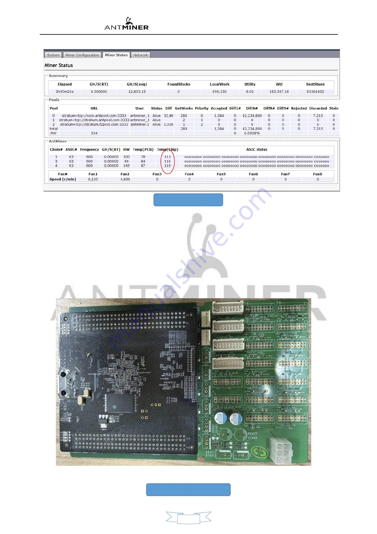
 31 No GH/S(RT)Red light Alarm 
 

Alarm phenomenon

Most are network exceptions

Temperature anomalies

Or the fan is abnormal. As you can see in the figure above

The sanbanxi 

temperature has exceeded Temp

chip

The upper limit and protect The alarm. In this case, please check the air volume of the Mining machine duct

Is there 

any blockage in the duct

Whether the fan is damaged

Whether there is dust in the tooth seam between the plate heatsink


2, non-Login monitoring interface

WEB

)。

 Including the mining machine.

I can't find it. IP


The majority of these phenomena are control Panel problems

Especially firmware reasons. Encounter this phenomenon

Restore factory Settings 

First

See if you can log in to the background properly

 If you can upgrade the firmware again. 


But there are two types of control panels

There are different ways to restore the factory settings. 

A C5 Control Panel

C5 The control Panel is made up of I Board and BB Board consisting of

),

As shown in figure 32 is shown

The other is 

XILINX

belong to one board

),

As shown in figure 33 is shown. 


 32

C5 Control system 


17


Summary of Contents for AntMiner S9

Page 1: ... 1 S9 is composed of 21 voltage domains connected in series There are 3 BM1387 chips in each voltage domain and there are 63 BM1387 chips in the whole board 2 The BM1387 has a built in buck diode with a step down diode function that is determined by the chip s designated pin 3 S9 is 21 voltage domains S5 is 16 voltage domains S7 54 chip is 18 voltage domains S7 45 is 15 voltage domains S9 clock is...

Page 2: ...is the voltage at the time of 1 8V When the operation is performed the voltage is also 1 8V when the operation is performed Purple for B BI BO Signal Flow 由 00 Number chip toward 62 Pull Low Level Not plugged in I Line Standby time is 0V When the operation is 0 3 Around the pulse signal Purple is B BI BO signal flow signal flow from 00 chip to chip to 62 low level no low level no low level no low ...

Page 3: ...ts on the front of the Operation board Note that Because the version of the S9 computing board is not exactly the same the LDO 1 8V power supply of the early voltage domains is powered by a separate peripheral LOD power supply chip for each of the three voltage domains The later version is changed to the internal chip Power supply BM1387 chip with 2 5 V input 1 8 V output LDO supply circuit except...

Page 4: ...uit diagram 6 BM1387 Chip Pin Signal Description Name I O Active Level Description 1 NRSTO O L Output to the chip of next level for the loop 2 BO O H Respond Busy Output 3 RI_A I N A Auxiliary Respond Input add diode and pulldown 4 Re I N A Respond Input Schmitt input and internal pullup 4 ...

Page 5: ...ge LDO 1 8V PLL 0 8V DC DCOutput andboost14VVoltage Detectionmethod 1 Do not Plug I O line Plug only 12V DC DC Output is Around 9v The boost output Voltage is around 14V Test points must have LCK 0 9V RI 1 8V Voltage Other test voltages is 0 2 Plug in I O when you do not press the test key DC DC No voltage output with boost after pressing the test key PIC Start working At this time DC DC Output PI...

Page 6: ...I Short or open circuit PLL 0 8 0 8 in When this voltage is abnormal the voltage domain has a chip PLL 08 Power supply short circuit or LDO 1 8 Abnormal LDO 2 5I 2 5 When this voltage is abnormal The chip LDO 2 5I Short or open circuit CORE 7 Chip peripheral test point and each voltage 3 According to the information on the diagnostics tool the operational state of the Operation board the chip arit...

Page 7: ...hould be to high level 6 7 8 A2 A1 A0 PIC Address signal 11 12 Txd RXD For the arithmetic board 3 3 End of the counting force of the channel After being divided by a resistor it becomes TX CO RX RI Signal I Port pin End ping du for 3 3v After the voltage is divided by the resistor Become a 1 8v 15 RST To reset the signal 3 3v After being divided by the resistor it becomes 1 8v in RST Reset Signal ...

Page 8: ... to 14 V The switching signal produced by U110 passes the output switch signal through L1 The switching signal produced by U110 passes the output switch signal through L1 for storage can inductance inductor a boost rectifier diode D100 and then C954 to charge and discharge whereby the discharge to thereby obtain a positive electrode C954 of 14 V Asshownin figure 11Figure 12 is shown 11 14V Boost s...

Page 9: ... board chip It also allows control of the operational DC DC Output voltage 13 PIC Schematic diagram 14 PIC 6 DC DCCircuit 由LM27402SQ与CMOS管TPHR9003NLCompositionFigure 15 below andFigure16isshown 15 DC DC Schematic diagram 9 PIC is running every minute we need to control the heartbeat signal if not With heartbeat information PIC will work for one minute and then shut down PIC pin 1 is VDD 3 3V 14 is...

Page 10: ...in 16 Pulse Pin 12 Switching signal Pin 11 Lower Bridge Drive Pin 14 Upper Bridge Drive DC DC When the voltage is abnormal First check through the fixture printing information to view PIC is the voltage value DC DC is the output voltage one to If there is a disagreement between Please change first LM27402SQ The small capacitance around If DC DC No output Please check R13 R14 Voltages 1v on both si...

Page 11: ...ltage domain s 3 A chip LDO The other is only the last 6 Voltage domain Setting External LDO The other voltages are built in by the chip LDO Provide yourself BM1387 Chips are Ready builtLDO Powersupply Circuit 由 BM1387 的14 LDO 25I pininput 10 脚 LDO 18th Output Andeachchip hasa separate LDO Non interference At last 6 Voltage domain LDO 25I The power supply is from 14V Boost circuit Other voltage do...

Page 12: ...formation screenshot Treatmentmethods Check the miner Light first If the miner s status is red a flashing flash Indicates that the mining machine is not in normal condition The mining machine network can be viewed first Use the computer to plug in the net of the mine machine internet line check Mine Pool of mining machine See is can and pass If the status of the indicator is normal The biggest pos...

Page 13: ... environment of the mining machine especially the ambient temperature for example in the winter in the north the mining machine has a high probability of sudden cooling Also check the network of the mining machine to the mine pool connection is unblocked This is also the case with external network instability If it doesn t work correctly after a reboot using a test fixture to test the three operat...

Page 14: ...use of failure Figure 24 can t find the 6th board Please check the IO cable corresponding to the 6th board The power cord is in good contact If there is no problem please use the test tool to perform single test on the 6th board If there is no problem please use the test tool to test the No 6 board Figure 25 can t find the No 1 board No 2 board has only 19 chips and it can t run Please check the N...

Page 15: ... as well as the static electricity in the environment If there is no static problem and the grounding is good please upgrade the latest firmware and use the tool to enter the board into the board 5 no GH S RT no GH S AVG red light flash As shownin Figure 28 28 only one fan is detected This phenomenon doesn t even have a temperature Can be seen from the above image Show only one fan The reason is t...

Page 16: ... As can be seen from the above figure The computing power of the 3rd board has reached 4791T This value is definitely not good because some signals on the No 3 computing board are incorrect and the control board accepts the information disorder Please use the test tool to perform a single test on the No 3 computing board If necessary please do a stress test compare the 550M computing board use the...

Page 17: ...etween the plate heatsink 2 non Login monitoring interface WEB Including the mining machine I can t find it IP The majority of these phenomena are control Panel problems Especially firmware reasons Encounter this phenomenon Restore factory Settings First See if you can log in to the background properly If you can upgrade the firmware again But there are two types of control panels There are differ...

Page 18: ...network indicator of the C5 control board is down as shown in Figure 34 below the network port of the XILINX control board is up as shown in Figure 35 below Reset 34 C5 Control Panel appearance Reset 35 XILINX Control Panel appearance The C5 control board is restored to the factory setting After the mining machine is running press and hold the RESET button for more than 5 seconds After the red lig...

Page 19: ...ooled Test the first block again So time just staggered Did not delay the total length of time 7 The repaired board Need to classify the fault and the replacement component model location reasons and other aspects of the record For feedback back to production after sale research and development 8 After the record Re installed into the whole machine for normal testing Fault type S9 Common fault typ...

Page 20: ... No or more than needed to U3 PIC Re upgrade Confirm PIC After the voltage is normal 检 测 U100 Whether there is output 15V Voltage Non detectable peripheral parts and U100 Itself 7Low Low calculation capacity can be divided into 1 When testing a box test The box received the Nuncio Enough Not enough power to show in the This phenomenon can be directly through the test box of the serial printing inf...

Reviews: