background image

21

Mar. 2011

RC-30

fig.b-JACK-2.eps

Summary of Contents for RC-30

Page 1: ...d View 1 6 Exploded View 1 Parts List 6 Exploded View 2 8 Exploded View 2 Parts List 9 Disassembly Procedure 9 Wiring Diagram Block Diagram 10 Parts List 12 Verifying the Version 14 Data Backup and Restore Operations 14 Performing a Factory Reset 14 Formatting the microSD Card 14 Updating the System 14 Test Mode 15 Circuit Board Jack DC Jack Board 20 Circuit Diagram Jack Board Digital 22 Circuit D...

Page 2: ...th an article on the market battery or etc Circuit Diagram In the circuit diagram UnPop is an abbreviation for Unpopulated This means non mounted components The circuit board and circuit board diagram show silk screened indications but no components are mounted Specifications RC 30 Loop Station Nominal Input Level MIC IN 40 dBu variable INST IN 20 dBu AUX IN 10 dBu Input Impedance MIC IN 4 kΩ INST...

Page 3: ...batteries cannot be used Current Draw Maximum 195 mA DC 9 V Expected battery life under continuous use Alkaline battery AA LR6 Approx 7 5 hours Carbon zinc battery AA R6 Approx 1 5 hours These figures will vary depending on the actual conditions of use Dimensions 173 W x 158 D x 57 H mm 6 13 16 W x 6 1 4 D x 2 1 4 H inches Weight 1 2 kg 2 lbs 11 oz including batteries Accessories Owner s Manual 51...

Page 4: ...4 Mar 2011 RC 30 Location of Controls fig panel eps 11 18 20 17 16 19 12 13 13 1 15 4 8 6 5 9 10 3 21 6 2 14 a a a a 7 b 5 ...

Page 5: ... 75D522N0R0 1 40128923 HEX NUT M7 1 5100018308 ROTARY POTENTIOMETER RD901F 40 125F A50K 00DQ8 1 11 75D422T1R0 PEDAL L 1 12 75D422T0R0 PEDAL R 1 13 5100008055 PEDAL PLATE 62X53 G2357116R0 2 14 5100018741 RUBBER SW 1 15 5100018738 REAR PANEL 1 16 F3449415R0 JACK KM02009BB 1 17 5100007092 USB CONNECTOR UBR24 4K5J00 F3439908R0 1 18 5100002907 6 5MM JACK HTJ 064 22H 5 5100008086 INT TOOTH WASHER 9 5X12...

Page 6: ...18R0 2 3 5100008056 BATTERY COVER G2017621R0 1 4 5100008058 TWIN BATTERY CASE V6 G2017620R0 1 5 5100008059 BATTERY TERMINAL G2177308R0 1 6 5100008061 BATTERY TERMINAL G2177309R1 1 7 5100008060 BATTERY TERMINAL G2177307R1 1 8 5100008057 BATTERY INSULATING SHEET G2257130R0 1 9 5100018870 BOTTOM LABEL 1 a 5100008245 SCREW 3X8 H5019115R0 PAN TAPPING B1 BZC 7 b 5100008243 SCREW 2 6X5 H5019430R0 BINDING...

Page 7: ...7 Mar 2011 RC 30 ...

Page 8: ...11 RC 30 Exploded View 2 fig bunkaizu e eps 1 4 1 2 9 3 5 8 7 6 10 23 14 12 21 13 19 22 15 16 20 25 24 26 18 b g b c f k i d e a h 20 11 LEFT SIDE RIGHT SIDE 17 Attach the wiring so that it is on the outer side ...

Page 9: ...17 LED GUIDE G2197126R0 1 16 5100018743 LED SPACER 1 17 04560601 CUSHION R G2357111 2 5100017360 JACK SHEET ASSY This unit includes the following parts 1 18 JACK BOARD 1 19 DC JACK BOARD 5100017361 PANEL SHEET ASSY This unit includes the following parts 20 PANEL BOARD 1 21 XLR BOARD 1 22 5100008055 PEDAL PLATE 62X53 G2357116R0 2 23 5100008054 PEDAL FOOT G2357115R0 2 24 5100007505 PEDAL GUIDE BUSH ...

Page 10: ...0 Wiring Diagram Block Diagram fig BLOCK eps L No Part Code Part Name Description Q ty 1 5100019608 WIRING W2 MAIN 1 2 5100019608 WIRING W2 MAIN 1 3 5100018920 WIRING W1 MIC 1 4 5100010465 WIRING 3P L 53X6X6MM P 2 0 1 ...

Page 11: ...11 Mar 2011 RC 30 fig BLOCK eps R ...

Page 12: ...BBER SW 1 SWITCH 5100011813 SWITCH F3159712R0 SV69010F 0202 6V NP 001 1 13129778 TACT SWITCH SKQKAHD010 2 JACK EXT TERMINAL 13449440R0 3 5MM JACK HSJ0857 016210 1 5100002907 6 5MM JACK HTJ 064 22H 5 F3449415R0 JACK KM02009BB 1 5100007092 USB CONNECTOR UBR24 4K5J00 F3439908R0 1 03459223 XLR CONNECTOR JY 5033A 1 PWB ASSY 5100017360 JACK SHEET ASSY 1 This unit includes the following parts JACK BOARD ...

Page 13: ...PLAIN WASHER 9X13 5X0 5T NI H5039158R0 5 MISCELLANEOUS 5100008055 PEDAL PLATE 62X53 G2357116R0 2 5100008237 PEDAL SHAFT H5029851R0 2 5100008052 BOTTOM FOOT G2357118R0 2 5100008059 BATTERY TERMINAL G2177308R0 1 5100008061 BATTERY TERMINAL G2177309R1 1 5100008060 BATTERY TERMINAL G2177307R1 1 5100018870 BOTTOM LABEL 1 5100007504 COIL SPRING 22177109R0 2 5100008057 BATTERY INSULATING SHEET G2257130R0...

Page 14: ... a factory reset is not possible Formatting the microSD Card When formatting the microSD card on the Main Board is necessary go to the owner s manual and refer to Formatting the Internal Memory p 17 Formatting the microSD card deletes the customer s data If necessary make a backup Updating the System Items Required Computer running Windows USB cable AC adaptor PSA series device Update program obta...

Page 15: ... down TAP TEMPO and or until one of the displays just described appears This takes approximately 2 seconds after the power is switched on Quitting the Test Mode Disconnect the plug from the OUTPUT L MONO jack Selecting or Skipping Test Items Selecting and executing a specific test item is not possible Skipping test items is also not possible Meanings of Error Codes 1 Version Check 1 Refer to Enter...

Page 16: ...ding on the 7 segment LED display changes as shown below r0 r1 r2 r3 r4 r5 r6 r7 r8 When the control is at center r4 is displayed When the values from MIN to MAX have been detected correctly execution automatically advances to the next test item 5 CTL PEDAL Test 1 Verify that F1 is shown on the 7 segment LED display 2 Depress the FS 5U connected to the FOOT SW jack tip end The reading on the 7 seg...

Page 17: ...annel 1 and channel 2 change Verify that the peak value is at 450 to 550 mVp p fig audio 5 eps 6 Disconnect the plugs from the INST IN L and R jacks 7 Input the following signal to the MIC IN connector using the DI 1 200 Hz sine wave at 200 mVp p 8 Make the following settings on the DI 1 ATT 0 dB Ø NOR GND NOR 9 Make the following settings on the oscilloscope Channel 1 OUTPUT L 2 00 V DIV 1 00 ms ...

Page 18: ...UTPUT R is at the following value Not more than 45 dBm JIS A or not more than 42 dBm DIN audio The value is raised by 40 dB internally by the DSP 3 Connect a CM 30 or a monitor amplifier to OUTPUT L and OUTPUT R and verify that no hum or shock noise is produced 4 Depress the left pedal to advance to the next test item 12 Factory Reset 1 Verify that FA is shown on the 7 segment LED display and that...

Page 19: ...19 Mar 2011 RC 30 ...

Page 20: ...20 Mar 2011 RC 30 Circuit Board Jack DC Jack Board fig b JACK 1 eps ...

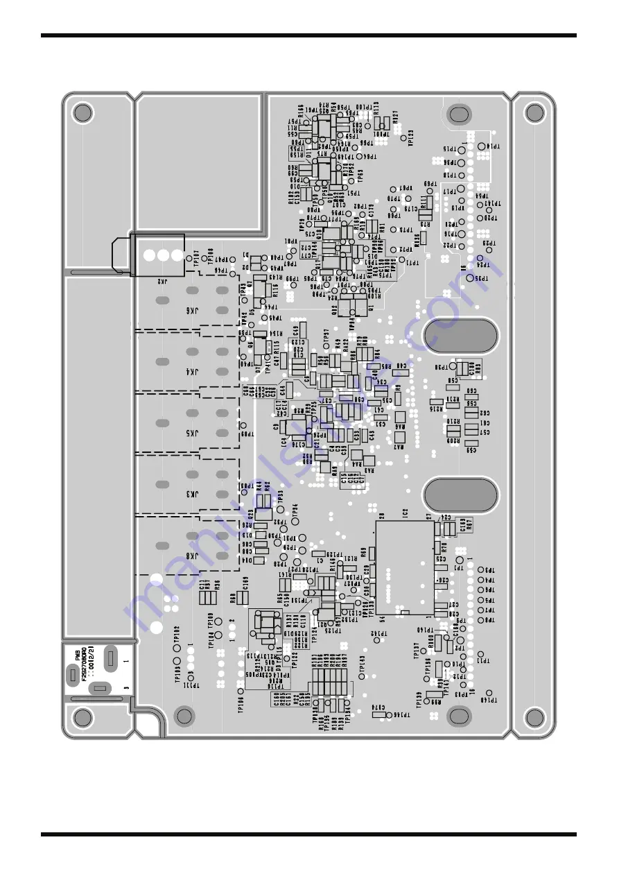
Page 21: ...21 Mar 2011 RC 30 fig b JACK 2 eps ...

Page 22: ...14 33 R15 33 R16 10 R17 100 R18 33 R20 0 1uF C2 0 1uF C3 1uF C4 10 R21 0 1uF C5 0 1uF C6 56k R28 0 1uF C10 UBR24 4K5J00 JK1 3 2 1 4 10 20 ACM2012 900 2P T002 L1 1 2 3 4 EZJZ1V500AA R34 EZJZ1V500AA R35 EZJZ1V500AA R36 R37 UnPop 1uF C11 0 1uF C12 0 1uF C13 10uF C7 10uF C8 0 1uF C14 0 1uF C15 10uF C16 10uF C17 D 0 5 12k R25 C19 UnPop C20 UnPop 0 R41 0 R40 C21 UnPop 10k R49 10k R50 R56 UnPop 33 R46 33...

Page 23: ... 29 A4 26 A3 10k R70 0 1uF C24 0 1uF C25 0 1uF C26 0 1uF C27 0 1uF C28 0 1uF C29 0 1uF C30 0 1uF C31 0 1uF C32 0 1uF C33 0 1uF C34 0 1uF C35 0 1uF C36 0 1uF C37 0 1uF C38 0 1uF C39 0 1uF C40 0 1uF C41 0 1uF C42 0 1uF C43 10uF C44 10uF C45 10uF C46 10uF C47 10uF C48 10uF C49 0 1uF C63 1uF C68 TC7WU04FU TE12L F IC7 6 2 22 R93 15pF C70 100 R80 0 1uF C64 680 R103 100 R79 0 1uF C66 100 R84 100 R78 22pF...

Page 24: ...22H JK6 1 3 4 2 100k R106 220pF C152 C115 10uF16V 100k R107 HSJ0857 0162109 JK2 1 3 2 1SS362FV TPL3 D2 2 3 1 C103 10uF16V 220pF C151 1SS362FV TPL3 D1 2 3 1 C113 10uF 16V D 0 5 10k R113 C111 10uF 16V D 0 5 12k R118 C93 10uF 16V D 0 5 10k R112 C153 UnPop R182 UnPop TP39 TP40 TP41 TP42 TP43 TP44 TP45 TP46 TP47 TP49 TP48 TP50 TP51 TP52 TP53 TP55 TP56 TP57 TP58 TP59 TP60 TP61 TP62 TP63 TP64 TP65 TP66 T...

Page 25: ...136 DTC114TUAT106 Q1 1 2 3 100k R109 D 0 5 10k R114 C82 10uF 16V 0 1uF C140 0 1uF C136 TP67 TP68 TP69 TP70 TP71 TP72 TP73 TP74 TP75 TP76 TP77 TP78 TP79 TP80 TP81 TP83 TP84 TP85 TP86 TP87 TP89 TP90 TP91 TP92 TP93 TP94 TP144 0 R94 0 R95 100k R97 1SS361FV TPL3 Z D15 3 2 1 D 0 5 10k R119 470k R19 470k R43 C126 10uF16V 100k R96 D 0 5 56k R58 D 0 5 56k R55 D 0 5 10k R162 D 0 5 10k R158 1800pF C125 1800p...

Page 26: ...0uF C144 0 1uF C156 0 1uF C155 0 047uF C139 0 047uF C143 0 047uF C138 0 01uF C51 0 01uF C135 D 0 5 1 5k R205 0 R191 D 0 5 5 6k R196 D 0 5 5 1k R168 0 01uF C52 0 R100 MCH6306 TL E Q9 3 G 1 D1 2 D2 5 D3 6 D4 4 S D24 RB160L 60 TE25 PB FREE 0 R39 0 R99 10k R138 TP136 TP139 TP137 TP134 TP135 TP138 TP142 TP143 TP146 TP148 0 1uF C137 0 R206 EZAEG3A50AV R207 WIRING RIBBON 3P AWG26 P2 0 CN5 1 2 3 WIRING RI...

Page 27: ...0 LT3482EUD TRPBF VIN 11 FSET 15 _SHDN 12 CTRL 13 NC 1 GND 9 GND 10 PAD 17 MON 16 APD 2 FB 14 VOUT1 5 VOUT2 4 MONIN 3 PUMP 6 SW 8 SW 7 4 7uF C117 0 1uF C100 TP123 TP124 TP125 TP126 TP127 TP128 2 2uF C108 50V 2 2uF C110 50V 2 2uF C109 50V TP129 TP130 TP131 TP132 TP133 0 R142 0 R141 NJM2882F33 TE1 IC9 1 VIN 3 CTRL 2 GND 4 N BP 5 VOUT 0 01uF C50 1uF C172 TP100 68uH CDRH4D28NP 680NC R L2 1uF C120 1uF ...

Page 28: ...28 Mar 2011 RC 30 Circuit Board Panel XLR Board fig b PANEL 1 eps ...

Page 29: ...29 Mar 2011 RC 30 fig b PANEL 2 eps ...

Page 30: ...W12 CARBON_SW BG603 02 11 21 22 12 SW13 CARBON_SW BG603 02 11 21 22 12 SW10 CARBON_SW BG603 03 11 21 22 12 SW11 CARBON_SW BG603 03 11 21 22 12 TP2 TP3 TP4 TP5 TP6 TP7 TP8 TP10 TP11 TP12 TP13 TP14 TP15 TP16 TP17 TP18 TP19 TP20 TP21 TP22 TP23 TP24 TP25 TP26 TP27 TP28 TP29 TP35 TP30 TP31 TP32 TP33 TP34 TP41 TP37 TP39 TP40 TP38 TP36 TP43 TP42 TP45 TP44 TP46 TP50 TP47 TP48 TP49 TP52 TP51 TP58 TP53 TP54...

Page 31: ...9 TP120 TP123 TP121 TP122 TP124 TP115 TP126 TP125 TP117 TP127 TP128 TP137 TP138 TP139 TP156 TP157 TP158 TP159 TP160 3 3k R51 3 3k R52 D 0 5 3 9k R54 D 0 5 3 9k R58 D 0 5 4 7k R63 D 0 5 4 7k R65 D 0 5 820 R78 D 0 5 4 7k R30 D 0 5 4 7k R28 220pF C6 100 R79 100 R80 10k R33 10k R34 220pF C7 220pF C8 D14 UnPop 2 3 1 TP161 TP162 TP163 L 34HDSL LED12 1 2 TP166 TP168 0 1uF C32 0 1uF C33 0 1uF C34 0 1uF C3...

Reviews: