background image

Broadcom

P411W-32P-UG104

14

P411W-32P PCIe 4.0 

User Guide 

NVMe Switch Adapter

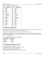
8.3  Electrical Characteristics

All power is supplied to the adapter through the PCIe 3.3V rails and the 12V rail. Onboard switching regulator circuitry that 
operates from the 3.3V rails and the 12V rail provides the necessary voltages. 

The supply voltages supplied by the PCIe edge connector are 12V ± 8% and 3.3V ± 9%.

Typical power is measured with maximum I/O traffic, typical silicon process material, and nominal voltages operating the 
card at an ambient temperature of 45°C with required airflow.The power requirements for the adapter under normal operation 
are shown in the following table.

8.4  Thermal and Atmospheric Limits

The atmospheric limits for the adapter are as follows:

Temperature range: 0°C to +55°C (+32°F to +131°F) (dry bulb)

Relative humidity range: 5% to 90% noncondensing

Maximum dew point temperature: 32°C (89.6°F)

Minimum airflow: 200 linear feet per minute at 55°C inlet temperature

A20

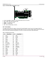
PERp0

B20

PETp0

A21

PERn0

B21

PETn0

A22

GND

B22

GND

A23

PERp1

B23

PETp1

A24

PERn1

B24

PETn1

A25

GND

B25

GND

A26

BP_TYPEB

B26

2W-CLKB

A27

2W_RESETB

B27

2W-DATAB

A28

GND

B28

GND

A29

B29

PERSTB#

A30

REFCLKB-

B30

CPRSNTB#

A31

GND

B31

GND

A32

PERp2

B32

PETp2

A33

PERn2

B33

PETn2

A34

GND

B34

GND

A35

PERp3

B35

PETp3

A36

PERn3

B36

PETn3

A37

GND

B37

GND

Table 8  P411W-32P NVMe Switch Adapter Power Consumption 

Power Mode

Typical Power

3.3V Supply

5.93W

+12V Supply

15.45W

Total Power

21.38W

Table 7  Internal Connector Pinout  (Continued)

Pin

Signal Name

Pin

Signal Name

Summary of Contents for P411W-32P

Page 1: ...Broadcom P411W 32P UG104 December 6 2019 P411W 32P PCIe 4 0 NVMe Switch Adapter User Guide Version 2 1...

Page 2: ...es For more information please visit www broadcom com Broadcom reserves the right to make changes without further notice to any products or data herein to improve reliability function or design Inform...

Page 3: ...ble Support 12 8 P411W 32P NVMe Switch Adapter Characteristics 12 8 1 LEDs 12 8 2 Physical Characteristics 12 8 2 1 Connectors 13 8 3 Electrical Characteristics 14 8 4 Thermal and Atmospheric Limits 1...

Page 4: ...e heartbeat LED and one system error status LED Complies with SFF TA 1005 Specification for Universal Backplane Management UBM 2 PCIe Interface PCIe is a high speed standard local bus for point to poi...

Page 5: ...through control of PERST timing Refer to the SFF TA 1005 Specification for Universal Backplane Management UBM for more UBM details 4 1 SFF TA 1005 UBM Based Backplanes Backplanes that use SFF TA 1005...

Page 6: ...s x4 connectors with one UBM target for each connector The red line indicates the I2 C bus connection 3 5 6 E X RIVE 3 5 6 E X RIVE 3 5 6 E X RIVE 3 5 6 E X RIVE SIDE 0 3LOT 3LOT 3LOT 3LOT 3 5 6 E X R...

Page 7: ...proper slot identification cables must connect based on the desired slot enumeration The most common backplane connector types are x4 or x8 SFF 8654 or SFF 8611 connectors Each x8 connector on the ada...

Page 8: ...o a given slot Figure 3 Backplane with x4 Connectors and VPP The following figure shows expected connections to a backplane that uses x8 SFF 8654 connectors from the adapter to NVMe drives by using VP...

Page 9: ...own resistor values on the adapter See Table 2 Sideband Management Pin Settings for the signal descriptions and see Table 7 Internal Connector Pinout for a complete connector pinout Table 1 Sideband S...

Page 10: ...two wire interface data signal PERST 0 Reset is asserted 1 Reset is not asserted The adapter drives the PCIe RESET signal This signal uses a clamp to ground so that the signal on the adapter powers u...

Page 11: ...Each connected drive is a port For example if two x4 NVMe drives connect to C0 one drive is on port 0 and the second drive is on port 4 as shown in the following table Use the same numbering schema i...

Page 12: ...cation Revision 3 0 The following figure shows the adapter board layout Table 5 Mixed Drive to Port Connection Example Adapter Label Tool Mapping Port Number Drive C0 C0 1 0 x2 2 x2 C0 0 4 x1 5 x1 6 x...

Page 13: ...9402 standard for connector sideband signal assignments Each x8 connector includes eight PCIe transmit and receive lanes and two sets of sidebands designated as A and B in accordance with the SFF 9402...

Page 14: ...4 Thermal and Atmospheric Limits The atmospheric limits for the adapter are as follows Temperature range 0 C to 55 C 32 F to 131 F dry bulb Relative humidity range 5 to 90 noncondensing Maximum dew p...

Page 15: ...mizes electromagnetic emissions susceptibility to radio frequency energy and the effects of electrostatic discharge The adapter model number 50054 meets the following integrated electromagnetic interf...

Page 16: ...standards CNS 13438 CNS15663 USA Canada Safety UL Listed For use with UL listed ITE equipment only Meets the following standards UL 60950 1 2nd Edition 2014 10 14 Information Technology Equipment Saf...

Page 17: ...s ESD safe set to a maximum torque of 4 8 0 5 inch pounds Replace the two Phillips screws removed in Step a ATTENTION Exceeding this torque specification can damage the board connectors or screws and...

Page 18: ...cables Replace the chassis cover reconnect any power cords and reconnect any network cables 10 Power on the system The hardware installation of your adapter is complete 11 Firmware Download Operation...

Page 19: ...updated Sideband Signals Added Connector Physical to Logical Mapping Updated Cable Support Updated Electrical Characteristics Added Firmware Download Operation Preliminary Version 1 2 September 26 201...

Page 20: ......

Reviews: