CHAPTER 4 DISASSEMBLY AND RE-ASSEMBLY
4-88
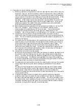
5. GUIDELINES FOR LEAD FREE SOLDER
Information on Manually Repairing PCB Soldered with Lead-Free Solder
This document provides information on how to correctly make manual repairs to a printed circuit
board (PCB) soldered with lead-free solder.
1. Characteristics of lead-free solder
Melting point higher than that of conventional tin-lead solder
(Lead-free solder: approx. 220'C, Conventional tin-lead solder: approx. 180'C)
Relatively poor solder wettability and spread (difficult to wet and spread), and hard
Appearance (dull and grainy surface) different from that of conventional solder
Relatively poor wettability, rough surface (bumps are likely to be formed), and solder
dragging
Poor solder elevation
Poor thermal conductivity and heat resistant (difficult to melt)
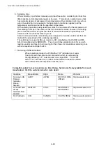
2. Metal composition & wire solder
The metal composition of lead-free solder allowed for use on PCBs for Brother's products is
following.
LF
Indication
Compositon
Manufacture
r
Origin Name
1
Sn/Ag/Cu
Nihon
Genma
Japan DHB-RMA3
NP303
H
only
Component-
side
Sn/Ag/Cu Nihon
Genma
Japan DHB-RMA3
NP303
We use wire solder which is indicated by digit after LF indication on PCB.
Wire solder made in the contries except Japan are under investigation,and will be evaluated.
3. Appearance quality criteria
The appearance of the surface of portions soldered with lead-free solder is basically the
same as that for those soldered with conventional lead-tin solder, except for the following
points.
1) The surface of a portion soldered with lead-free solder is dull and not smooth.
2) Shrinkage cracks can be observed on the surface of a portion soldered with lead-free
solder. (They can be observed using a magnifying glass with approx. 10x
magnification.)
Shrinkage
cracks
Figure 1 Shrinkage Cracks
4. Identification of lead-free solder on PCBs
For PCBs that use lead-free solder, "LF" is indicated by silk-screen printing or attaching a
label. "LF" stands for lead free and indicates that the PCBs bearing such an indication have
been soldered with lead-free solder. A digit is given in a box following "LF" if produced by
silk-screen printing or follows "LF" without a box on an attached label, the digit indicating the
metal composition and wire solder.
Summary of Contents for DCP-8040
Page 276: ...CHAPTER 7 MAINTENANCE MODE 7 6 Fig 7 3 l m a b c d e f g h i j k ...
Page 347: ...APPENDIX 4 CIRCUIT DIAGRAMS A 50 Appendix 4 1 Main PCB Circuit Diagram 1 7 ...
Page 349: ...APPENDIX 4 CIRCUIT DIAGRAMS A 52 Appendix 4 3 Main PCB Circuit Diagram 3 7 ...
Page 351: ...APPENDIX 4 CIRCUIT DIAGRAMS A 54 Appendix 4 5 Main PCB Circuit Diagram 5 7 ...
Page 353: ...APPENDIX 4 CIRCUIT DIAGRAMS A 56 Appendix 4 7 Main PCB Circuit Diagram 7 7 ...
Page 355: ...APPENDIX 4 CIRCUIT DIAGRAMS A 58 Appendix 4 9 Engine PCB Circuit Diagram 1 2 ...
Page 357: ...APPENDIX 4 CIRCUIT DIAGRAMS A 60 Appendix 4 11 NCU PCB Circuit Diagram U S A ...
Page 359: ...APPENDIX 4 CIRCUIT DIAGRAMS A 62 Appendix 4 13 NCU PCB Circuit Diagram Asia ...
Page 361: ...APPENDIX 4 CIRCUIT DIAGRAMS A 64 Appendix 4 15 Control Panel PCB Circuit Diagram ...
Page 367: ...April 04 SM FAX027 5 8C5903 Printed in Japan ...


