APPENDIX 3 FIRMWARE SWITCHS (WSW)
A-16
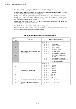
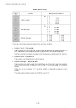
WSW09 (Protocol definition 1)
Selector
No.
Function
Setting and Specifications
1
Frame length selection
0: 256 octets
1: 64 octets
2
Use of non-standard commands
0: Allowed
1: Prohibited
3
4
No. of retries
No. 3
4
0
0
:
4
times
0
1
:
3
times
1
0
:
2
times
1
1
:
1
time
5
T5 timer
0: 300 sec.
1:
60 sec.
6
T1 timer
0: 35 sec.
1:
40 sec.
7
8
Elapsed time for time-out
control for no response from the
called station in automatic
sending mode
No. 7 8
0
0
: 60 sec.
(55 sec. for US and Canada)
0
1
:
140
sec.
1
0
: 90 sec.
1
1
: 35 sec.
NOTE:
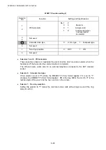
Selectors 1 through 6 are not applicable in those models which do not support ECM.
l
Selector 1: Frame length selection
Usually a single frame consists of 256 octets (1 octet = 8 bits). For communications lines
with higher bit error rate, however, set selector 1 to "1" so that the machine can divide a
message into 64-octet frames.
Remarks:
The error correction mode (ECM) is a facsimile transmission manner in which
the machine divides a message into frames for transmission so that if any data
error occurs on the transmission line, the machine retransmits only those frames
containing the error data.
l
Selector 2: Use of non-standard commands
If this selector is set to "0," the machine may use non-standard commands (the machine’s
native-mode commands, e.g., NSF, NSC, and NSS) for communications. If it is set to "1,"
the machine will use standard commands only.
l
Selectors 3 and 4: No. of retries
These selectors set the number of retries in each specified modem transmission speed.
l
Selector 5: T5 timer
This selector sets the time length for the T5 timer.
l
Selector 6: T1 timer
This selector sets the time length for the T1 timer.
l
Selectors 7 and 8: Elapsed time for time-out control
If the machine receives no response (no G3 command) from the called terminal in automatic
sending during the time set by these selectors, it disconnects the line.
Summary of Contents for DCP-8040
Page 276: ...CHAPTER 7 MAINTENANCE MODE 7 6 Fig 7 3 l m a b c d e f g h i j k ...
Page 347: ...APPENDIX 4 CIRCUIT DIAGRAMS A 50 Appendix 4 1 Main PCB Circuit Diagram 1 7 ...
Page 349: ...APPENDIX 4 CIRCUIT DIAGRAMS A 52 Appendix 4 3 Main PCB Circuit Diagram 3 7 ...
Page 351: ...APPENDIX 4 CIRCUIT DIAGRAMS A 54 Appendix 4 5 Main PCB Circuit Diagram 5 7 ...
Page 353: ...APPENDIX 4 CIRCUIT DIAGRAMS A 56 Appendix 4 7 Main PCB Circuit Diagram 7 7 ...
Page 355: ...APPENDIX 4 CIRCUIT DIAGRAMS A 58 Appendix 4 9 Engine PCB Circuit Diagram 1 2 ...
Page 357: ...APPENDIX 4 CIRCUIT DIAGRAMS A 60 Appendix 4 11 NCU PCB Circuit Diagram U S A ...
Page 359: ...APPENDIX 4 CIRCUIT DIAGRAMS A 62 Appendix 4 13 NCU PCB Circuit Diagram Asia ...
Page 361: ...APPENDIX 4 CIRCUIT DIAGRAMS A 64 Appendix 4 15 Control Panel PCB Circuit Diagram ...
Page 367: ...April 04 SM FAX027 5 8C5903 Printed in Japan ...

