Confidential
2-25
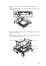
(13) Assemble the FG harness FB with the one cup S M3x6 Taptite screw.
(14) Assemble the FG harness ADF with the one cup S M3x6 Taptite screw.
Note:
Make sure to place the Harness of the connector CN1 and CN2 on the back of the Driver
PCB shield.
Fig. 2-40
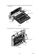
(15) Connect the three Connectors (CN1, CN2, CN5) into the Driver PCB ASSY.
Fig. 2-41
Driver PCB ASSY
<Left side>
CN5
CN2
CN1
Driver PCB ASSY
FG harness ADF
Taptite, cup S M3x6
Taptite, cup S M3x6
FG harness FB
<Left side>
Document scanner unit
Driver PCB shield
Document scanner unit
CN1
CN2
Summary of Contents for DCP-9040CN
Page 309: ...Confidential 4 5 8 Alert warning message of WHQL appears Click Continue Anyway to proceed ...
Page 325: ...Confidential 5 6 Color scanning Fig 5 2 ...
Page 342: ...Confidential 5 23 Cover page sample Fig 5 13 End page sample Fig 5 14 ...
Page 365: ...Confidential 6 2 Charge High voltage Power Supply PCB Circuit Diagram 2 4 ...
Page 366: ...Confidential 6 3 Charge High voltage Power Supply PCB Circuit Diagram 3 4 ...
Page 367: ...Confidential 6 4 Charge High voltage Power Supply PCB Circuit Diagram 4 4 ...
Page 368: ...Confidential 6 5 Transfer High voltage Power Supply PCB Circuit Diagram 1 2 ...
Page 369: ...Confidential 6 6 Transfer High voltage Power Supply PCB Circuit Diagram 2 2 ...
Page 370: ...Confidential 6 7 Low voltage Power Supply PCB Circuit Diagram 100V ...
Page 371: ...Confidential 6 8 Low voltage Power Supply PCB Circuit Diagram 200V ...
Page 373: ...Confidential 6 10 Filter PCB Circuit Diagram ...


