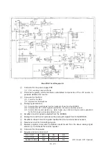
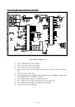
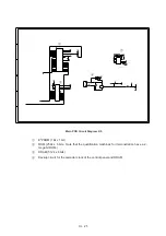
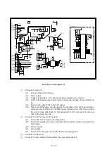
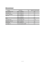
III –
26
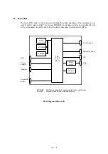
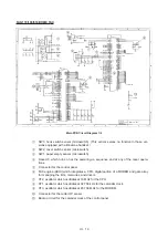
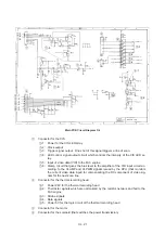
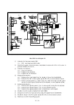
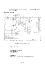
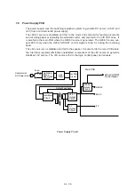
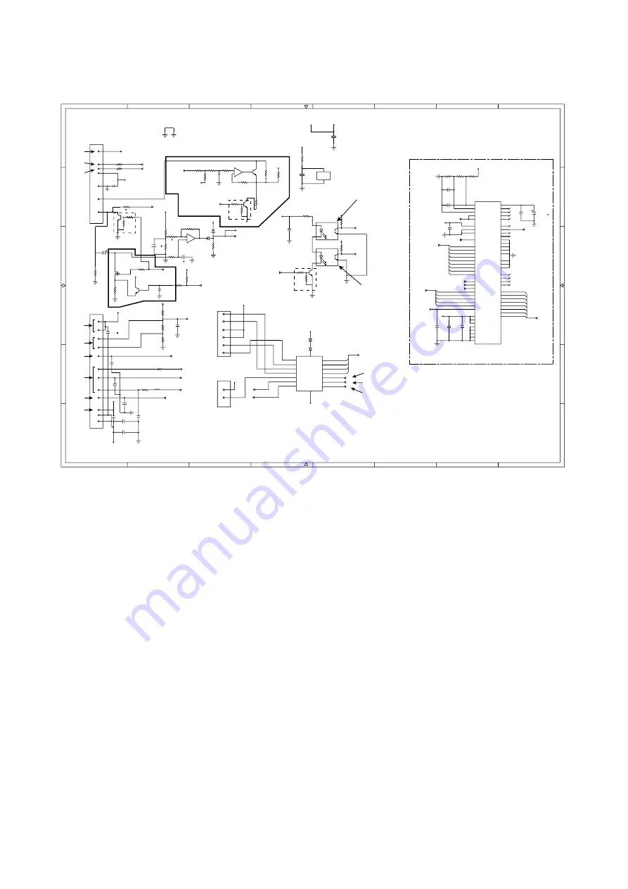
Main PCB Circuit Diagram 3/5
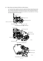
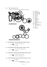
1
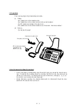
Connector for the CIS
1
-1: Power for the CIS LED array
1
-2: Clock output
1
-3: Trigger signal output. One shot of this signal triggers a line of scan.
1
-4: LED control signal output circuit which controls the intensity of the CIS LED ar-
ray.
1
-5: Input of video data (VID) to the FAX engine
1
-6: Clamp circuit that gives the bias level to the amplifier of the VID input circuit ac-
cording to the CLAMP and CLPWM signals issued by the CPU (that monitors
the current video data input) for compensating the DC component of video sig-
nals for the next scan line
2
Connector for the thermal recording head
2
-1: Power 26V for the thermal recording head
2
-2: Thermister signals which are normalized by the resistor network and fed to the
FAX engine
2
-3: Strobe signals
2
-4: Data signals
2
-5: Power 5V for the logic circuit of the thermal recording head
3
Connector for the motor
4
Connector for the solenoid (that switches the power transmission)
+
26V
R B
1 3 E
1 3 D
1 3 D
G N D
+ 5
C I S
P 7
B 7 B P H
1
3
9
5
4
T M
3
7
8
P 8
B 1 2 B P H
R 1 0 5
3 3 K F
R 1 0 6
1 0 0 K F
T G
1 3 E
7
2
6
2
1 0
D O U T
1 3 D
1
R 1 1 2
1 2
6
R 1 0 8
8 . 2 K F
R 1 2 6
7 5 0
R 1 2 3
7 5 0
R S T H
A T A P
P O R T 0
P O R T 1
A I N
T E M P
T R I G
P D 6 / S D C K
C L K 2
P D 4 / P P 4
D A C K / P P 7
D 7
D 6
D 5
D 4
D 3
D 2
D 1
D 0
4 2
3 9
4 0
3 1
3 4
3 3
4 7
4 8
5 1
5 2
5 3
5 7
6 0
2 7
2 2
2 1
2 5
1
2
3
4
1
2
3
4
# 1 5
L C 8 2 1 0 2
1 7 B
1 9
A 3
A 2
A 1
1 6
1 8
2 3
5 4
5 5
S H
6 3
D R E Q / P P 6
5 8
M T P / P P 5
5 9
I C L K
I O C S
M C S
I O E
M E
R D
3 7
R S T L
A D R E F L
3 8
3 6
4 6
A G N D
A G N D
A 0
M M 1
D 7
D 6
D 5
D 4
M M 4
M M 3
M M 2
P O R T 3
S A M P
P D 7 / S D
1 5 A
R S T L
A 3
A 2
A 1
C K 1 6
I O R Q
R D
W R
M R E Q
1 3 D
S M C
A V D D
A 0
W R
C L K I N
R E S E T
V D D
V D D
V D D
D G N D
D G N D
D G N D
D G N D
D G N D
R0
V
R 1 2 2
1 5 0
C 9 9
1 0 4
C 1 0 7
1 0 4
R 1 2 8
7 5
R 1 3 3
3 9 0
+ R 5
V I D
3 3 C , 3 2 B
4 3
T G
3 2 B
S B U S
C 1 0 2
1 0 4
+ R 5
R0
V
2 0
1 3 D
E 1 C S
1 6 E
S R A M
3 0
2 9
2 8
A 7
A B U S
A 7
A 6
A 5
1 1
1 3
1 4
1 5
A 4
1 2
A 8
1 7 D
A 4
A 8
A 6
A 5
1 7 C
2 4
5 6
9
1 7
2 6
4 9
6 4
C
110
104
C
100
104
C9
6
102B
G N D
P O R T 2
P D 5 / S D E
P D 3 / P P 3
P D 2 / P P 2
P D 1 / P P 1
P D 0 / P P 0
C L K 1
R S
C 1 0 5
1 0 4
C 1 0 5
1 6 V
1 0
R 0 V
R D A T
1 6 C
5 0
GN
D
6 1
6 2
M B U S
1
2
3
4
5
6
P 4
B 6 B P H
0 1
0 2
0 3
0 4
0 5
0 6
0 7
I N 1
I N 2
I N 3
I N 4
I N 5
I N 6
I N 7
+ 2 6 V
+ 2 6 V
1
2
4 2 A
4 1 E
P O N
C M L L
P 3
B 2 B P H
# 1 2
T D 6 2 0 0 3 P
1 6
1 5
1 4
1 3
1 2
1 1
1 0
D B U S
8
D 1
D 2
D 3
D 0
1 4 E
5
6
7
1 3 E
1 6 D
1 6 D
5
6
7
S O L
P W O N
C M L H
P 0 V
8
G N D
Z D 3
M T Z J 8 . 2
Z D 4
M T Z J 8 . 2
+ 2 6 V
.9
C O M
4 1
4 5
4 4
3 5
3 2
1 0
+ 5
+R
5
R 0 V
C 1 0 1
1 0 4
Q 1 1
D 2 0 9 6
R 1 3 6
N C
R 1 2 7
1 0 0
R 1 1 5
5 6 K
R 1 1 7
3 . 3 K
1 3 B
L I G T
R 1 2 0
2 . 2 K
C 9 8
1 0 4
+5
G N D
R 1 3 1
1 0 0
R 1 3 5
1 / 4 W
1 8
R 1 2 9
1 W
2 7
Q 1 3
D T D
1 1 3 Z K
L O N
1 6 D
P 0 V
* R 1 1 6
0
V I D
3 7 B
* Q 1 0
R 0 V
* C 9 7
N C
N C
R
119
10K
R 0 V
D
S
G
*
R
118
NC
* Q 9
N C
+ R 5
* R 1 1 0
N C
C L A M P
1 6 D
G N D
* C 9 5
N C
* R 1 1 4
N C
C L P W M
1 6 D
* R 1 1 1
N C
+ 5
*
C
104
NC
*
R
124
0
* R 1 2 1
N C
+ R 5
* R 1 3 4
0
* R 1 3 7
N C
5
6
# 1 6
N J M 2 1 1 4
R 0 V
1
2
* R 1 2 5
N C
* C 1 0 3
C 9 0
R
1 M
R 0 V
* Z D 5
N C
* D 6
N C
+ R 5
* R 1 3 2
N C
R 0 V
V I D
V I D
3 7 B
1 3 C
R 0 V
G N D
+ 5
+ R 5
C
109
104
R 0 V
+ 2 6 V
R 1 3 0
8 2 0
1 / 2 W
R 0 V
C 1 0 8
1 0 4
+ 5
1 3 E
1 3 D
+ 5
+ 5
+ 2 6 V
C 5 6
G N D
N C
R 6 2
1 / 2 W
2 . 4 K
S G - 1 0 5 F 3 0 8
P H 1
S G - 1 0 5 F 3 0 8
P H 2
1 3 E
S E O N
Q 3
G N D
K R C 1 0 7 S
G N D
R 3 0
1 0 0 K
R E A R
R 3 7
1 0 0 K
F R N T
4
5
1 1
H 2 6 V
R 0 V
C P 3 I
1 2 E
C 9 3
1 0 2 B
G N D
S T 2
1 3 D
C 9 4
1 0 2 B
1 0 0
1 3 D
D I N
C 8 1
1 0 0 P
R 9 8
1 5 0
L 1 4
M M Z Y 6 0 1 B
H D C
S T 1
C 8 5
1 0 2 B
GN
D
+ 5
C 9 1
1 0 4
C 8 8
1 0 4
C 8 7
N C
P 0 V
G N D
C 8 3
1 0 0 P
# 1 6
N J M 2 1 1 4
8
4
M O T O R
S O L
7
1
2
3
# 1 6
N J M 2 1 1 4
0
Not mounted.
* Q 8
N C
1
2
3
4
5
6
7
8
2
1
3
4
5
6
7
8
A
B
C
D
E
F
A
B
C
D
E
F
+
-
+
-
1
1
-1
1
-2
1
-3
1
-6
1
-4
1
-5
3
4
5
6
6
-1
6
-2
5
-1
5
-2
5
-3
5
-4
2
-1
2
-2
2
-3
2
-4
2
-3
2
-5
2
Summary of Contents for FAX-270MC
Page 4: ...CHAPTER I GENERAL DESCRIPTION ...
Page 11: ...CHAPTER II INSTALLATION ...
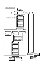
Page 12: ...CHAPTER III THEORY OF OPERATION ...
Page 49: ...CHAPTER IV DISASSEMBLY REASSEMBLY AND LUBRICATION ...
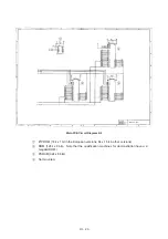
Page 86: ...IV 36 4 Cutter unit Cutter unit A A A A ...
Page 87: ...CHAPTER V MAINTENANCE MODE ...
Page 140: ...CHAPTER VI ERROR INDICATION AND TROUBLESHOOTING ...
Page 157: ...March 98 5X1S112 Printed in Japan ...
Page 173: ...D POWER SUPPLY 100 120 V U S A CANADA ...
Page 174: ...POWER SUPPLY 200 240 V EUROPE SOUTH AMERICA D ...
Page 175: ...POWER SUPPLY 200 240 V GULF ASIA CHINA D ...
Page 192: ...D POWER SUPPLY 100 120 V U S A CANADA ...
Page 193: ...POWER SUPPLY 200 240 V EUROPE SOUTH AMERICA D ...
Page 194: ...POWER SUPPLY 200 240 V GULF ASIA CHINA D ...
Page 195: ...FACSIMILE EQUIPMENT PARTS REFERENCE LIST MODEL FAX170 190 190 Plus 195 ...
Page 198: ......
Page 203: ......
Page 206: ...Remarks 8 8 8 8 8 8 9 9 8 8 8 8 8 8 0 1 0 1 Brother Technical Information FAX98250 4 ...
Page 208: ... 8 01 8 01 8 8 8 8 0 1 0 1 8 8 8 8 Brother Technical Information FAX99102 6 ...
Page 220: ......