VI
- 11
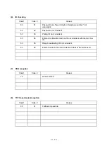
(9)
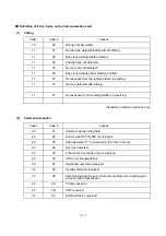
Signal isolation
Code 1
Code 2
Causes
90
01
Unable to detect video signals and commands within 6 seconds
after CFR is transmitted.
90
02
Received PPS containing invalid page count or block count.
(10) Video signal reception
Code 1
Code 2
Causes
A0
03
Error correction sequence not terminated even at the final
transmission speed for fallback.
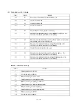
A0
11
Receive buffer empty. (5-second time-out)
A0
12
Receive buffer full during operation except receiving into
memory.
A0
13
Decoding error continued on 500 lines.
A0
14
Decoding error continued for 10 seconds.
A0
15
Time-out: Five seconds or more for one-line transmission.
A0
16
RTC not found and carrier OFF signal detected for 6 seconds.
A0
17
RTC found but no command detected for 60 seconds.
A0
18
Receive buffer full during receiving into memory.
A8
01
RTN, PIN, or ERR received at the calling terminal.*
A9
01
RTN, PIN, or ERR received at the called terminal.*
* Available in German versions only
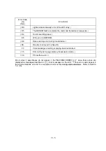
(11) General communications-related
Code 1
Code 2
Causes
B0
02
Unable to receive the next-page data.
B0
03
Unable to receive polling even during turn-around transmission
due to call reservation.
B0
04
PC interface error.
Summary of Contents for FAX-8650P
Page 1: ...FACSIMILE EQUIPMENT SERVICE MANUAL MODEL FAX3750 FAX 8650P MFC7750 ...
Page 5: ...CHAPTER I GENERAL DESCRIPTION ...
Page 12: ...CHAPTER II INSTALLATION ...
Page 13: ...CONTENTS 1 INSTALLING THE UPDATE DATA TO THE FACSIMILE EQUIPMENT II 1 ...
Page 16: ...CHAPTER III THEORY OF OPERATION ...
Page 18: ...III 1 1 OVERVIEW Not provided on the FAX 8650P ...
Page 28: ...III 11 Not provided on the FAX 8650P Location of Sensors and Actuators ...
Page 31: ...III 14 Main PCB Modem PCB ...
Page 36: ...CHAPTER IV DISASSEMBLY REASSEMBLY AND LUBRICATION ...
Page 42: ...IV 4 n n Disassembly Order Flow ...
Page 71: ...IV 33 1 Provided on the FAX 8650P 2 Not provided on the FAX 8650P ...
Page 72: ...IV 34 Setting up the main PCB after replacement ...
Page 84: ...IV 46 2 Control panel locks 3 Scanner frame ASSY and separation roller gear ...
Page 85: ...IV 47 4 Top cover lock spring 5 Gear drive unit ...
Page 86: ...CHAPTER V MAINTENANCE MODE ...
Page 93: ...V 6 Scanning Compensation Data List ...
Page 141: ...V 54 FAX3750 FAX 8650P MFC7750 Key Button Entry Order ...
Page 146: ...CHAPTER VI ERROR INDICATION AND TROUBLESHOOTING ...
Page 171: ...Oct 98 SM5X5303 Printed in Japan ...
Page 172: ...FAX3750 FAX 8650P MFC7750 Appendix 1 EEPROM Customizing Codes ...
Page 194: ......
Page 195: ......
Page 196: ......

