CHAPTER 3 THEORY OF OPERATION
3-7
1.3
Main PCB
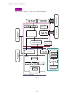
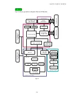
For the entire circuit diagram of the main PCB, see
Appendix 11 to 17
.
1.3.1
ASIC
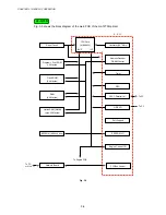
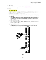
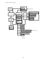
A Fujitsu 32bit RISC CPU, MB86833 (SPARC lite) is built in the ASIC. While the CPU is driven
with a clock frequency of 33 MHz in the user logic block, it itself runs at 66 MHz, which is
generated by multiplying the source clock by two.
The functions of the interface block communication with external devices are described below;
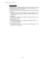
(1) IEEE1284
Stores the data received from the PC into DRAM as controlled by the DMA controller. It is
applicable to both normal receiving and bi-directional communication (nibble mode, byte
mode, ECP mode).
(2) USB interface (for HL-1240 only)
Stores the data received from the PC into DRAM as controlled by the DMA controller. The
transmission speed is 12Mbps.
(3) Engine GA transfer circuit
Communicates with the engine GA by a full-duplex synchronous serial method. The
communication speed is 2Mbps.
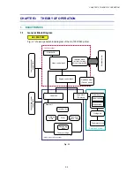
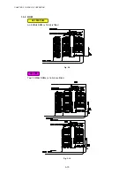
Fig. 3-7
HL-1030/1240
Summary of Contents for HL-1030
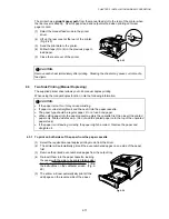
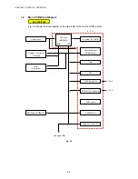
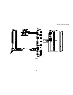
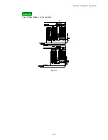
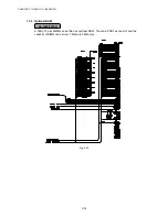
Page 51: ...CHAPTER 3 THEORY OF OPERATION 3 9 Fig 3 8 ...
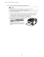
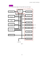
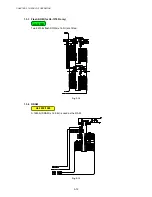
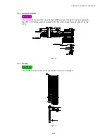
Page 53: ...CHAPTER 3 THEORY OF OPERATION 3 11 Two 32 Mbits ROMs x 16 bit are fitted Fig 3 11 HL 1270N ...
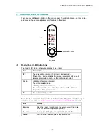
Page 122: ...CHAPTER 5 PERIODIC MAINTENANCE 5 8 ...
Page 198: ...CODE UK4352000 B512040CIR 1 2 A 20 NAME Appendix 11 Main PCB Circuit Diagram HL 1030 1240 1 2 ...
Page 199: ...Appendix 12 Main PCB Circuit Diagram HL 1030 1240 2 2 CODE UK4352000 B512040CIR 2 2 A 21 NAME ...
Page 202: ...CODE UK4361000 B512049CIR A 24 NAME Appendix 15 Main PCB Circuit Diagram HL 1250 1270N 3 5 ...
Page 205: ...Appendix 18A Engine PCB Circuit Diagram OLD CODE UK4444000 B512059CIR A 27 NAME ...
Page 206: ...Appendix 18B Engine PCB Circuit Diagram NEW CODE UK4444000 B512059CIR A 28 NAME ...
Page 207: ...Appendix 19 Network Board Circuit Diagram HL 1270N CODE LJ8107000 B512058CIR A 29 NAME ...
Page 218: ...INDEX vi ...

