VI
- 5
10
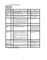
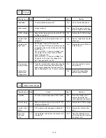
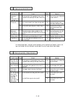
No
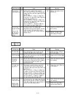
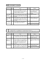
Development
input signal error
Do the pins 3, 4 and 5 of the connector
P6 on the main PCB have the following value
respectively when a sheet of paper is fed from
the MP tray?
P6-3 pin (DBAC) --- Change in voltage from
6V approx. to 0V just when a sheet of paper is
fed from the registration unit.
P6-4 pin (DBDC) --- Change in voltage from
9V approx. to 0V just when a sheet of paper is
fed from the registration unit.
P6-5 pin (DNSTY) --- Change in voltage to
2.5V just when a sheet of paper is fed.
Replace the scanner unit or
the harness.
Possible cause
Step
Check
Result
Remedy
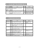
Dirt on power
supply terminal
Failure in the
development
high-voltage
circuit
Is there any dirt on the cartridge side
development terminal of the transfer unit and
on the terminal of the high-voltage power
supply development unit? (is there continuity
between them?)
11
No
Clean the contacts to assure
the continuity.
Yes
Replace the high-voltage
power supply PCB assy.
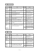
1
Yes
Density setting
Does printed image improve when density
setting is changed on the control panel?
Adjust the proper setting on
the control panel.
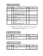
I-2
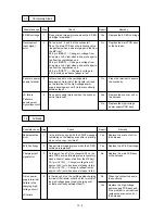
Dark
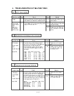
Possible cause
Step
Check
Result
Remedy
EP-ED cartridge
Is there any dirt on the cartridge side charging
terminal of the transfer unit and on the terminal
of the high-voltage power supply charging unit?
(is there continuity between them?)
5
No
Clean the terminal to assure
the continuity.
Yes
Replace the high-voltage
power supply PCB assy.
2
Does printed image improve when the EP-ED
cartridge is replaced?
Yes
Replace the EP-ED cartridge.
Dirt on the
grounding
terminal
3
Does printed image improve when continuity
is improved by cleaning the EP-ED cartridge
grounding terminal and the printer unit
grounding terminal?
Yes
Clean the contacts to assure
the continuity.
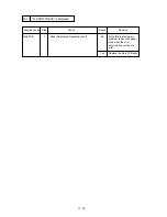
Charging input
signal error
4
Do the pins 1, 2 and 5 of the connector P6
on the main PCB have the following value
respectively when a sheet of paper is fed from
the MP tray?
P6-1 pin (HV1AC) --- Change in voltage from
6V approx. to 0V just when a sheet of paper is fed.
P6-2 pin (HV1DC) --- Change in voltage from
9V approx. to 0V just when a sheet of paper is fed.
P6-5 pin (DNSTY) --- Change in voltage to
2.5V just when a sheet of paper is fed.
No
Replace the main PCB assy
or the harness.
Dirt on power
supply terminal
Failure in the
charging high-
voltage circuit
Summary of Contents for HL-1260
Page 1: ...SERVICE MANUAL MODEL HL 1260 R LASER PRINTER ...
Page 40: ...III 8 K D E F A C 2 C 3 C C 1 J B G 2 G 1 G H I Figure 3 6 Main PCB Circuit ...
Page 109: ...Appendix 3 Main PCB Circuitry Diagram 1 8 A 3 CODE NAME UK2495000 B48K158 159CIR 1 8 ...
Page 110: ...Appendix 4 Main PCB Circuitry Diagram 2 8 A 4 CODE NAME UK2495000 B48K158 159CIR 2 8 ...
Page 111: ...Appendix 5 Main PCB Circuitry Diagram 3 8 A 5 CODE NAME UK2495000 B48K158 159CIR 3 8 ...
Page 112: ...Appendix 6 Main PCB Circuitry Diagram 4 8 A 6 CODE NAME UK2495000 B48K158 159CIR 4 8 ...
Page 113: ...Appendix 7 Main PCB Circuitry Diagram 5 8 A 7 CODE NAME UK2495000 B48K158 159CIR 5 8 ...
Page 114: ...Appendix 8 Main PCB Circuitry Diagram 6 8 A 8 CODE NAME UK2495000 B48K158 159CIR 6 8 ...
Page 115: ...Appendix 9 Main PCB Circuitry Diagram 7 8 A 9 CODE NAME UK2495000 B48K158 159CIR 7 8 ...
Page 116: ...Appendix 10 Main PCB Circuitry Diagram 8 8 A 10 CODE NAME UK2495000 B48K158 159CIR 8 8 ...
Page 117: ...Appendix 11 Control Panel PCB Circuitry Diagram 1 1 A 11 CODE NAME UK2527000 B48K143CIR ...
Page 118: ...Appendix 12 Scanner LD PCB Circuitry Diagram 1 1 A 12 CODE NAME UK2674000 B48K165CIR ...
Page 119: ...SERVICE MANUAL MODEL HL 1260e 1660 R LASER PRINTER ...
Page 144: ...III 7 Figure 3 6 Main PCB Circuit A C 2 C 3 C J K B I H 1 H 2 C 1 H G G 1 G 2 F E D ...
Page 168: ...CODE UK3268000 B48K259 235CIR 1 7 NAME Appendix 3 Main PCB Circuitry Diagram 1 7 ...
Page 169: ...CODE UK3268000 B48K259 235CIR 2 7 NAME Appendix 4 Main PCB Circuitry Diagram 2 7 A 3 ...
Page 170: ...CODE UK3268000 B48K259 235CIR 3 7 NAME Appendix 5 Main PCB Circuitry Diagram 3 7 A 4 ...
Page 171: ...CODE UK3268000 B48K259 235CIR 4 7 NAME Appendix 6 Main PCB Circuitry Diagram 4 7 A 5 ...
Page 172: ...CODE UK3268000 B48K259 235CIR 5 7 NAME A 6 Appendix 7 Main PCB Circuitry Diagram 5 7 ...
Page 173: ...CODE UK3268000 B48K259 235CIR 6 7 NAME Appendix 8 Main PCB Circuitry Diagram 6 7 A 7 ...
Page 174: ...CODE UK3268000 B48K259 235CIR 7 7 NAME Appendix 9 Main PCB Circuitry Diagram 7 7 A 8 ...
Page 175: ...CODE UK3253000 B48K253CIR 1 1 NAME Appendix 11 Scanner LD PCB Circuitry Diagram 1 1 A 9 ...
Page 188: ...PARTS REFERENCE LIST MODEL HL 1260e R LASER PRINTER ...
Page 213: ...I Brother Laser Printer HL 1260e HL 1660 USER S GUIDE ...
Page 422: ...USER S GUIDE Appendix 16 PC 8 10U PC 8 D N 11U PC 850 12U PC 852 17U ...
Page 423: ...APPENDICES Appendix 17 PC 8 Turkish 9T Windows Latin1 19U Windows Latin2 9E Windows Latin5 5T ...
Page 424: ...USER S GUIDE Appendix 18 Legal 1U Ventura Math 6M Ventura Intl 13J Ventura US 14J ...
Page 425: ...APPENDICES Appendix 19 PS Math 5M PS Text 10J Math 8 8M Pi Font 15U ...
Page 426: ...USER S GUIDE Appendix 20 MS Publishing 6J Windows 3 0 9U Desktop 7J MC Text 12J ...
Page 429: ...APPENDICES Appendix 23 PC 8 PC 8 D N PC 850 PC 852 ...
Page 430: ...USER S GUIDE Appendix 24 PC 860 PC 863 PC 865 PC 8 Turkish ...
Page 431: ...APPENDICES Appendix 25 IBM Mode PC 8 PC 8 D N PC 850 PC 852 ...
Page 432: ...USER S GUIDE Appendix 26 PC 860 PC 863 PC 865 PC 8 Turkish ...
Page 433: ...APPENDICES Appendix 27 HP GL Mode ANSI ASCII 9825 CHR SET ...
Page 434: ...USER S GUIDE Appendix 28 FRENCH GERMAN SCANDINAVIAN SPANISH LATIN JIS ASCII ...
Page 435: ...APPENDICES Appendix 29 ROMAN8 EXT ISO IRV ISO SWEDISH ISO SWEDISH N ...
Page 436: ...USER S GUIDE Appendix 30 ISO NORWAY 1 ISO GERMAN ISO FRENCH ISO U K ...
Page 437: ...APPENDICES Appendix 31 ISO ITALIAN ISO SPANISH ISO PORTUGUESE ISO NORWAY 2 ...

