VI-18
5.
TROUBLESHOOTING PAPER TRANSPORT PROBLEMS
5.1 Paper
Jams
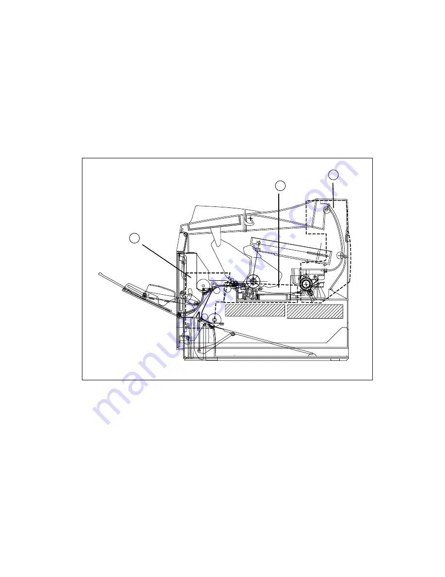
The paper path is divided into following three blocks:
1)
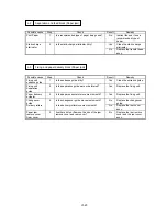
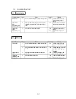
The paper pick-up block, (The LCD display "JAM TRAYS")
2)
The separation and feed block, (The LCD display "JAM INSIDE")
3)
The fixing and paper delivery block, (The LCD display "JAM REAR")
Therefore, remedies for paper jam problems are described.
Respectively for these three blocks.
Figure 6.3
3
2
1
Summary of Contents for HL-2060
Page 1: ...MECHANICS ELECTRONICS SERVICE MANUAL LASER PRINTER ...
Page 41: ...III 8 A B F C D E 1 E 2 E 3 E 4 E 5 F Figure 3 7 Paper Feed Size SW PCB Circuit ...
Page 129: ...VII 16 Test for memory MEMORY DISPLAY MEMORY DEBUG MEMORY TEST exit MENU ...
Page 137: ...Appendix A 3 Main PCB Circuitry Diagram 1 7 CODE UK4058000 B512006 CIR 1 7 NAME A 3 ...
Page 138: ...Appendix A 4 Main PCB Circuitry Diagram 2 7 CODE UK4058000 B512006 CIR 2 7 NAME A 4 ...
Page 139: ...Appendix A 5 Main PCB Circuitry Diagram 3 7 CODE UK4058000 B512006 CIR 3 7 NAME A 5 ...
Page 140: ...Appendix A 6 Main PCB Circuitry Diagram 4 7 CODE UK4058000 B512006 CIR 4 7 NAME A 6 ...
Page 141: ...Appendix A 7 Main PCB Circuitry Diagram 5 7 CODE UK4058000 B512006 CIR 5 7 NAME A 7 ...
Page 142: ...Appendix A 8 Main PCB Circuitry Diagram 6 7 CODE UK4058000 B512006 CIR 6 7 NAME A 8 ...
Page 143: ...Appendix A 9 Main PCB Circuitry Diagram 7 7 CODE UK4058000 B512006 CIR 7 7 NAME A 9 ...
Page 144: ...Appendix A 10 Control Panel PCB Circuitry Diagram 1 1 CODE UK4077000 B512005 CIR NAME A 10 ...
Page 145: ...Appendix A 11 Laser LD PCB Circuitry Diagram 1 1 CODE UK3253000 B48K253 CIR NAME A 11 ...
Page 147: ...June 98 54T046NE0 HL2060 ...


