VI-23
(8)
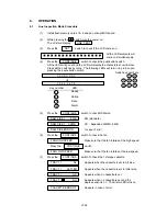
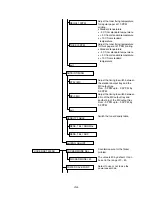
Press the CONTINUE switch to check the 2nd stage cassette.
TRAY 2 = A4
Appears when the cassette is set to A4 size.
TRAY 2 = LETTER
Appears when the cassette is set to letter size.
TRAY 2 = NO
Appears when no cassette is set.
CASSETTE ERROR!!
Appears in case of error.
(9)
Press the CONTINUE switch to check multi purpose tray.
MP TRAY
Set paper on the MP tray.
MP TRAY OK!!
(10)
Stuck sensor check
STUCK = LOW
Appears when the stuck full sensor for the
standard output tray is off.
STUCK = FULL
Appears when the stuck full sensor for the
standard output tray is on.
(11)
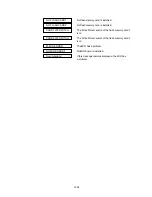
Press the CONTINUE switch to check flash memory cards and the MIO.
CARD1 R/W START
Checks reading/writing on Card 1 ID.
È
CARD1 R/W OK!!
The flash card works correctly.
È
CARD2 R/W START
Checks reading/writing on Card 2 ID.
È
CARD2 R/W OK!!
The flash card works correctly.
È
MIO CHECK START
The flash card works correctly.
È
RAM SIZE = 8M
È
Now initializing
È
LJ WAIT 001P T1
È
LJ READY 001P T1
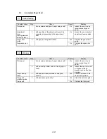
(13) Turn off the power.
Note: The checks on and after (11) are carried out automatically, and if an error
is detected, on of the following messages will be displayed.
Checks can be resumed if the CONTINUE switch is pressed.
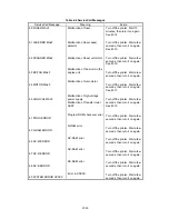
R/W ERROR CARD1
There is a problem in reading/writing from the
flash memory card 1.
R/W ERROR CARD2
There is a problem in reading/writing from the
flash memory card 2.
You can turn off the power when this message is
displayed. If there is no toner cartridge or paper, the
message "14 NO CARTRIDGE" or “CHECK TRAY”
will be displayed.
Summary of Contents for HL-2060
Page 1: ...MECHANICS ELECTRONICS SERVICE MANUAL LASER PRINTER ...
Page 41: ...III 8 A B F C D E 1 E 2 E 3 E 4 E 5 F Figure 3 7 Paper Feed Size SW PCB Circuit ...
Page 129: ...VII 16 Test for memory MEMORY DISPLAY MEMORY DEBUG MEMORY TEST exit MENU ...
Page 137: ...Appendix A 3 Main PCB Circuitry Diagram 1 7 CODE UK4058000 B512006 CIR 1 7 NAME A 3 ...
Page 138: ...Appendix A 4 Main PCB Circuitry Diagram 2 7 CODE UK4058000 B512006 CIR 2 7 NAME A 4 ...
Page 139: ...Appendix A 5 Main PCB Circuitry Diagram 3 7 CODE UK4058000 B512006 CIR 3 7 NAME A 5 ...
Page 140: ...Appendix A 6 Main PCB Circuitry Diagram 4 7 CODE UK4058000 B512006 CIR 4 7 NAME A 6 ...
Page 141: ...Appendix A 7 Main PCB Circuitry Diagram 5 7 CODE UK4058000 B512006 CIR 5 7 NAME A 7 ...
Page 142: ...Appendix A 8 Main PCB Circuitry Diagram 6 7 CODE UK4058000 B512006 CIR 6 7 NAME A 8 ...
Page 143: ...Appendix A 9 Main PCB Circuitry Diagram 7 7 CODE UK4058000 B512006 CIR 7 7 NAME A 9 ...
Page 144: ...Appendix A 10 Control Panel PCB Circuitry Diagram 1 1 CODE UK4077000 B512005 CIR NAME A 10 ...
Page 145: ...Appendix A 11 Laser LD PCB Circuitry Diagram 1 1 CODE UK3253000 B48K253 CIR NAME A 11 ...
Page 147: ...June 98 54T046NE0 HL2060 ...

