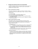
II-5
3.
IMAGE FORMATION SYSTEM
3.1 Outline
The image formation system is the main part of the printer. The print information, after
input from the video controller circuit into the engine controller circuit as a TVDO signal,
forms a toner image on the photosensitive drum.
Then the toner image is transferred onto the paper by the transfer charging roller. The
image formation system is composed of the photosensitive drum the charging unit, the
developing unit and the cleaning unit.
3.2 Printing
Process
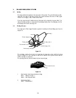
The major part of the image formation system is contained in the cartridge, as shown in
Figure 2.5.
Figure 2.5
The cartridge used by the printer has a seamless photosensitive drum with the structure
shown in Figure 2.6. The outer layer of the drum consists of an organic photoconductor
(OPC); the base is aluminum.
The printing process can be divided into five major stages:
Figure 2.6
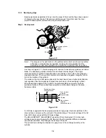
1.
Electrostatic latent image formation stage
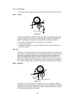
Step 1 Primary charge (-)
Step 2 Scanning exposure
2. Developing
stage
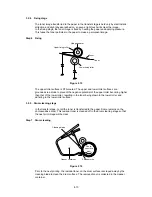
Step 3 Development
Photoconductive layer
Base
Laser beam
Developing cylinder
Primary charging roller
Cleaning blade
Photosensitive drum
Static charge eliminator
Cartridge
Transfer charging roller
Blade
Paper
Summary of Contents for HL-2060
Page 1: ...MECHANICS ELECTRONICS SERVICE MANUAL LASER PRINTER ...
Page 41: ...III 8 A B F C D E 1 E 2 E 3 E 4 E 5 F Figure 3 7 Paper Feed Size SW PCB Circuit ...
Page 129: ...VII 16 Test for memory MEMORY DISPLAY MEMORY DEBUG MEMORY TEST exit MENU ...
Page 137: ...Appendix A 3 Main PCB Circuitry Diagram 1 7 CODE UK4058000 B512006 CIR 1 7 NAME A 3 ...
Page 138: ...Appendix A 4 Main PCB Circuitry Diagram 2 7 CODE UK4058000 B512006 CIR 2 7 NAME A 4 ...
Page 139: ...Appendix A 5 Main PCB Circuitry Diagram 3 7 CODE UK4058000 B512006 CIR 3 7 NAME A 5 ...
Page 140: ...Appendix A 6 Main PCB Circuitry Diagram 4 7 CODE UK4058000 B512006 CIR 4 7 NAME A 6 ...
Page 141: ...Appendix A 7 Main PCB Circuitry Diagram 5 7 CODE UK4058000 B512006 CIR 5 7 NAME A 7 ...
Page 142: ...Appendix A 8 Main PCB Circuitry Diagram 6 7 CODE UK4058000 B512006 CIR 6 7 NAME A 8 ...
Page 143: ...Appendix A 9 Main PCB Circuitry Diagram 7 7 CODE UK4058000 B512006 CIR 7 7 NAME A 9 ...
Page 144: ...Appendix A 10 Control Panel PCB Circuitry Diagram 1 1 CODE UK4077000 B512005 CIR NAME A 10 ...
Page 145: ...Appendix A 11 Laser LD PCB Circuitry Diagram 1 1 CODE UK3253000 B48K253 CIR NAME A 11 ...
Page 147: ...June 98 54T046NE0 HL2060 ...

