II-9
3.2.3 Transfer
stage
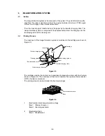
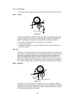
In the transfer stage, the toner image is transferred from the drum surface to the paper.
Step 4 Transfer
Photo-
sensitive
drum
Paper
Transfer charging roller
Figure 2.13
A positive charge applied to the back of the paper attracts the negatively charged toner
particles to the paper. The printer accomplishes transfer by using the charging roller
method. Advantages compared with the corona transfer method are as follows:
•
Low transfer voltage that is less than half that for corona transfer.
•
Less ozone generation.
•
The paper is supported by the transfer charging roller and photosensitive drum, so
feed is more stable.
Reference:
If the image on the photosensitive drum is not completely transferred to the paper due to
jamming, etc., the toner may adhere to the transfer charging roller. The printer removes
the toner from the transfer charging roller by switching the transfer voltage between
positive and negative in sequence. During wait, initial rotation, and last rotation, the
printer sets the primary DC voltage to zero, and sets the charge on the drum to zero. In
this case, the transfer voltage is made negative to remove the negatively-charged toner
on the transfer charging roller to the drum. The transfer charging roller is thus cleaned.
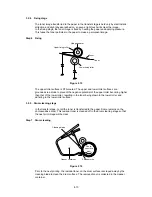
Step 5 Separation
Photo-
sensitive
drum
Paper
Transfer charging roller
Static charge
eliminator
Figure 2.14
The stiffness of the paper causes it to separate from the drum. (Curvature separation)
To stabilize the paper feed and prevent small white circles from appearing in the printed
image at low temperature and humidity, the charge on the back of the paper is reduced
by the static charge eliminator after transfer.
Summary of Contents for HL-2060
Page 1: ...MECHANICS ELECTRONICS SERVICE MANUAL LASER PRINTER ...
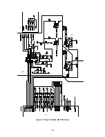
Page 41: ...III 8 A B F C D E 1 E 2 E 3 E 4 E 5 F Figure 3 7 Paper Feed Size SW PCB Circuit ...
Page 129: ...VII 16 Test for memory MEMORY DISPLAY MEMORY DEBUG MEMORY TEST exit MENU ...
Page 137: ...Appendix A 3 Main PCB Circuitry Diagram 1 7 CODE UK4058000 B512006 CIR 1 7 NAME A 3 ...
Page 138: ...Appendix A 4 Main PCB Circuitry Diagram 2 7 CODE UK4058000 B512006 CIR 2 7 NAME A 4 ...
Page 139: ...Appendix A 5 Main PCB Circuitry Diagram 3 7 CODE UK4058000 B512006 CIR 3 7 NAME A 5 ...
Page 140: ...Appendix A 6 Main PCB Circuitry Diagram 4 7 CODE UK4058000 B512006 CIR 4 7 NAME A 6 ...
Page 141: ...Appendix A 7 Main PCB Circuitry Diagram 5 7 CODE UK4058000 B512006 CIR 5 7 NAME A 7 ...
Page 142: ...Appendix A 8 Main PCB Circuitry Diagram 6 7 CODE UK4058000 B512006 CIR 6 7 NAME A 8 ...
Page 143: ...Appendix A 9 Main PCB Circuitry Diagram 7 7 CODE UK4058000 B512006 CIR 7 7 NAME A 9 ...
Page 144: ...Appendix A 10 Control Panel PCB Circuitry Diagram 1 1 CODE UK4077000 B512005 CIR NAME A 10 ...
Page 145: ...Appendix A 11 Laser LD PCB Circuitry Diagram 1 1 CODE UK3253000 B48K253 CIR NAME A 11 ...
Page 147: ...June 98 54T046NE0 HL2060 ...


