III-2
1.2
Video Controller Circuit
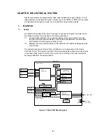
(1) CPU
block
CPU(#33) MB86832-100 manufactured by Fujitsu
RISC chip
Clock speed: 33.1768 Mhz (3 times faster than the base clock)
Appearance: 178-pin QFP
Voltage: 3V
(2)
ASIC/Gate Array Block
•
#19 MB87F1611(Fujitsu) - 240-pin QFP
Controls the address decoder, timers and interfaces (Centronics and RS-232C).
•
Controls HRC(High Resolution Control), GSC(Gray Scale Control) and
economy mode, drivened by 3V.
•
#2 µPD65632GC - 100-pin QFP
Controls the I/O ports and others.
(3)
Font Card Block
•
Font Card (option)
The font card has a 64MB memory area and is controlled by the 16-bit bus.
The card is supplied with 12V power in the slot 2 because the PCMCIA card
requires 12V power supply when writing or erasing data.
The address bus is buffered by LS245 and the data bus, is buffered by
LCX245.
(4)
Centronics/RS-232C interface block
•
Centronics parallel interface
Data transmission and reception are controlled by the MB87F1611 (#19).
•
RS-232C
Data transmission and reception are controlled by the MB87F1611 (#19).
The ADM202JRN (#35) serves as driver/receiver.
(5) SIMM
block
•
SIMM (Single-Inline-Memory-Module) allows memory extension up to 72MB
•
2 SIMM sockets are available.
•
SIMM should be of 72-pin type and its access time should be less than 70 ns.
•
12 types of SIMM (1MB, 2MB, 4MB, 8MB, 16MB and 32MB) can be combined:
1MB MH25632BJ-7 (MITSUBISHI), HB56D25632B-7A (HITACHI)
2MB MH51232BJ-7 (MITSUBISHI), HB56D51232B-7A (HITACHI)
4MB MH1M32EJ-7 (MITSUBISHI), HB56A132BT-7A (HITACHI)
8MB MH2M32EJ-7 (MITSUBISHI), HB56A232BT-7A (HITACHI)
16MB THM324000BSG-60, -70, -80 (TOSHIBA)
32MB THM328020BSG-60, -70, -80 (TOSHIBA)
Note:
Fast page type and EDO type can be used together although it is not
recommended.
1) The SIMMs have its printed marking on the PCB by silk screen: SLOT1 and
SLOT2, respectively.
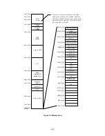
2) The attached Printer SIMM map shows the memory map for 4 SIMMs combined.
Summary of Contents for HL-2060
Page 1: ...MECHANICS ELECTRONICS SERVICE MANUAL LASER PRINTER ...
Page 41: ...III 8 A B F C D E 1 E 2 E 3 E 4 E 5 F Figure 3 7 Paper Feed Size SW PCB Circuit ...
Page 129: ...VII 16 Test for memory MEMORY DISPLAY MEMORY DEBUG MEMORY TEST exit MENU ...
Page 137: ...Appendix A 3 Main PCB Circuitry Diagram 1 7 CODE UK4058000 B512006 CIR 1 7 NAME A 3 ...
Page 138: ...Appendix A 4 Main PCB Circuitry Diagram 2 7 CODE UK4058000 B512006 CIR 2 7 NAME A 4 ...
Page 139: ...Appendix A 5 Main PCB Circuitry Diagram 3 7 CODE UK4058000 B512006 CIR 3 7 NAME A 5 ...
Page 140: ...Appendix A 6 Main PCB Circuitry Diagram 4 7 CODE UK4058000 B512006 CIR 4 7 NAME A 6 ...
Page 141: ...Appendix A 7 Main PCB Circuitry Diagram 5 7 CODE UK4058000 B512006 CIR 5 7 NAME A 7 ...
Page 142: ...Appendix A 8 Main PCB Circuitry Diagram 6 7 CODE UK4058000 B512006 CIR 6 7 NAME A 8 ...
Page 143: ...Appendix A 9 Main PCB Circuitry Diagram 7 7 CODE UK4058000 B512006 CIR 7 7 NAME A 9 ...
Page 144: ...Appendix A 10 Control Panel PCB Circuitry Diagram 1 1 CODE UK4077000 B512005 CIR NAME A 10 ...
Page 145: ...Appendix A 11 Laser LD PCB Circuitry Diagram 1 1 CODE UK3253000 B48K253 CIR NAME A 11 ...
Page 147: ...June 98 54T046NE0 HL2060 ...

