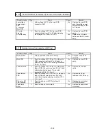
VI-5
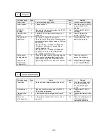
Possible cause
Step
Check
Result
Remedy
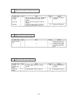
Development
input signal
error
10
Do the pins 3, 4 and 5 of the connector
P6 on the main PCB have the following value
respectively when a sheet of paper is fed from
the MP tray?
P6-3 pin (DBAC) --- Change in voltage from
6V approx. to 0V just when a sheet of paper is
fed from the registration unit.
P6-4 pin (DBDC) --- Change in voltage from
9V approx. to 0V just when a sheet of paper is
fed from the registration unit.
P6-5 pin (DNSTY) --- Change in voltage to
2.5V just when a sheet of paper is fed.
No
Replace the laser unit or
the harness.
Dirt on power
supply terminal
11
Is there any dirt on the cartridge side
development terminal of the transfer unit and
on the terminal of the high-voltage power
No
Clean the contacts to
assure the continuity.
Failure in the
development
high-voltage
circuit
supply development unit? (is there continuity
between them?)
Yes
Replace the high-voltage
power supply PCB assy.
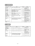
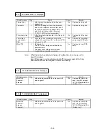
I-2 Dark
Possible cause
Step
Check
Result
Remedy
Density setting
1
Does printed image improve when density
setting is changed on the control panel?
Yes
Adjust the proper setting
on the control panel.
EP-ED HC
cartridge
2
Does printed image improve when the EP-ED
HC cartridge is replaced?
Yes
Replace the EP-ED HC
cartridge.
Dirt on the
grounding
terminal
3
Does printed image improve when continuity
is improved by cleaning the EP-ED HC
cartridge grounding terminal and the printer
unit grounding terminal?
Yes
Clean the contacts to
assure the continuity.
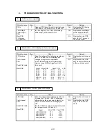
Charging input
signal error
4
Do the pins 1, 2 and 5 of the connector P6
on the main PCB have the following value
respectively when a sheet of paper is fed from
the MP tray?
P6-1 pin (HV1AC) --- Change in voltage from
6V approx. to 0V just when a sheet of paper is
fed.
P6-2 pin (HV1DC) --- Change in voltage from
9V approx. to 0V just when a sheet of paper is
fed.
P6-5 pin (DNSTY) --- Change in voltage to
2.5V just when a sheet of paper is fed.
No
Replace the main PCB
assy or the harness.
Dirt on power
supply terminal
5
Is there any dirt on the cartridge side charging
terminal of the transfer unit and on the terminal
of the high-voltage power supply charging unit?
No
Clean the terminal to
assure the continuity.
Failure in the
charging high-
voltage circuit
(is there continuity between them?)
Yes
Replace the high-voltage
power supply PCB assy.
Summary of Contents for HL-2060
Page 1: ...MECHANICS ELECTRONICS SERVICE MANUAL LASER PRINTER ...
Page 41: ...III 8 A B F C D E 1 E 2 E 3 E 4 E 5 F Figure 3 7 Paper Feed Size SW PCB Circuit ...
Page 129: ...VII 16 Test for memory MEMORY DISPLAY MEMORY DEBUG MEMORY TEST exit MENU ...
Page 137: ...Appendix A 3 Main PCB Circuitry Diagram 1 7 CODE UK4058000 B512006 CIR 1 7 NAME A 3 ...
Page 138: ...Appendix A 4 Main PCB Circuitry Diagram 2 7 CODE UK4058000 B512006 CIR 2 7 NAME A 4 ...
Page 139: ...Appendix A 5 Main PCB Circuitry Diagram 3 7 CODE UK4058000 B512006 CIR 3 7 NAME A 5 ...
Page 140: ...Appendix A 6 Main PCB Circuitry Diagram 4 7 CODE UK4058000 B512006 CIR 4 7 NAME A 6 ...
Page 141: ...Appendix A 7 Main PCB Circuitry Diagram 5 7 CODE UK4058000 B512006 CIR 5 7 NAME A 7 ...
Page 142: ...Appendix A 8 Main PCB Circuitry Diagram 6 7 CODE UK4058000 B512006 CIR 6 7 NAME A 8 ...
Page 143: ...Appendix A 9 Main PCB Circuitry Diagram 7 7 CODE UK4058000 B512006 CIR 7 7 NAME A 9 ...
Page 144: ...Appendix A 10 Control Panel PCB Circuitry Diagram 1 1 CODE UK4077000 B512005 CIR NAME A 10 ...
Page 145: ...Appendix A 11 Laser LD PCB Circuitry Diagram 1 1 CODE UK3253000 B48K253 CIR NAME A 11 ...
Page 147: ...June 98 54T046NE0 HL2060 ...


