II-3
1.2
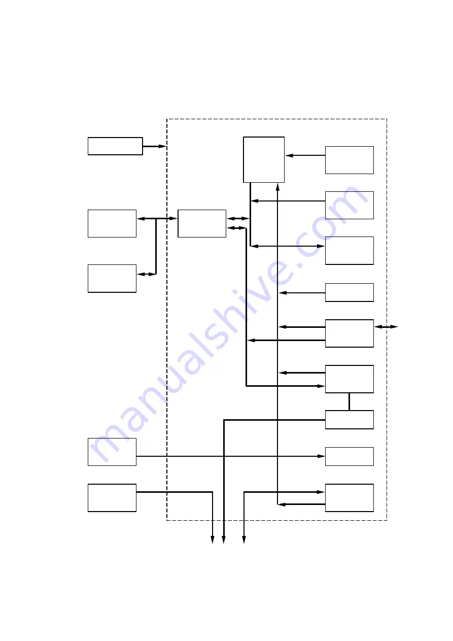
Main PCB Block Diagram
<HL-720>
Fig. 2.3 shows a block diagram of the main PCB.
Reset Circuit
DRAM
0.5 Mbytes
Option RAM
1.5 Mbytes or
3.5 Mbytes
EEPROM
(128 x 8 bits)
DRAM Control
Oscillator
(12.27 MHz)
Program ROM
16 Kbytes
Working S-RAM
512 Bytes
Timer
CDCC
Parallel I/O
DATA
Extension
FIFO
EEPROM I/O
Engine
Control I/O
To Panel sensor PCB
To PC
ASIC
CPU Core
(Z80)
BUS
INT
Motor Driver
Fig. 2.3
Summary of Contents for HL-720
Page 1: ...SERVICE MANUAL MODEL HL 720 730 730Plus R LASER PRINTER ...
Page 36: ...II 19 1 3 10 Engine I O HL 720 Fig 2 21 shows the engine interface circuit Fig 2 21 ...
Page 37: ...II 20 HL 730 730Plus Fig 2 22 shows the engine interface circuit Fig 2 22 ...
Page 61: ... Fig 3 18 2 4 1 1 1 ...
Page 92: ...SERVICE MANUAL MODEL HL 760 R LASER PRINTER ...
Page 109: ...II 8 1 3 4 DRAM Two 4M bit DRAMs x 16bits are used as the RAM Fig 2 6 ...
Page 113: ...II 12 1 3 10 Engine I O Fig 2 12 shows the engine interface circuit Fig 2 12 ...
Page 114: ...II 13 1 3 11 Paper Feed Motor Drive Circuit Fig 2 13 ...
Page 133: ...Appendix 2 Main PCB Circuit Diagram 1 3 CODE UK3227000 B48K272CIR 1 3 NAME ...
Page 134: ...Appendix 3 Main PCB Circuit Diagram 2 3 CODE UK3227000 B48K272CIR 2 3 NAME ...
Page 135: ...CODE UK3227000 B48K272CIR 3 3 NAME Appendix 4 Main PCB Circuit Diagram 3 3 ...


