II-6
<HL-730/730Plus>
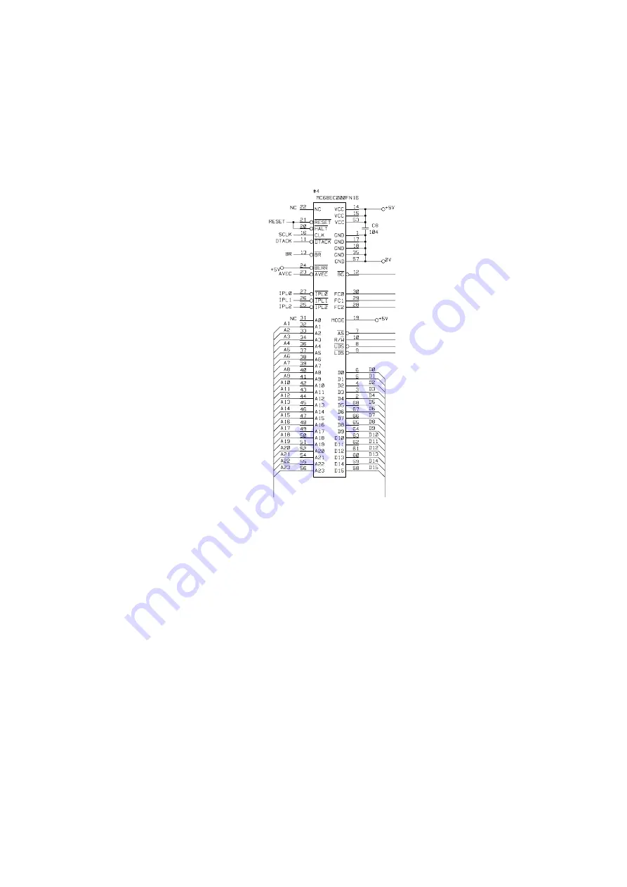
Fig. 2.6. shows the CPU circuit block on the main PCB.
The CPU is a Motorola MC68EC000FN16 which is driven with a clock frequency of
15.3 MHz. This clock frequency is made by dividing the source clock of 30.67 MHz
into two. The address bus is 23 bits of A1 to A23, and the data bus is 16 bits. The total
memory space is 16 Mbytes.
Fig. 2.6
Summary of Contents for HL-720
Page 1: ...SERVICE MANUAL MODEL HL 720 730 730Plus R LASER PRINTER ...
Page 36: ...II 19 1 3 10 Engine I O HL 720 Fig 2 21 shows the engine interface circuit Fig 2 21 ...
Page 37: ...II 20 HL 730 730Plus Fig 2 22 shows the engine interface circuit Fig 2 22 ...
Page 61: ... Fig 3 18 2 4 1 1 1 ...
Page 92: ...SERVICE MANUAL MODEL HL 760 R LASER PRINTER ...
Page 109: ...II 8 1 3 4 DRAM Two 4M bit DRAMs x 16bits are used as the RAM Fig 2 6 ...
Page 113: ...II 12 1 3 10 Engine I O Fig 2 12 shows the engine interface circuit Fig 2 12 ...
Page 114: ...II 13 1 3 11 Paper Feed Motor Drive Circuit Fig 2 13 ...
Page 133: ...Appendix 2 Main PCB Circuit Diagram 1 3 CODE UK3227000 B48K272CIR 1 3 NAME ...
Page 134: ...Appendix 3 Main PCB Circuit Diagram 2 3 CODE UK3227000 B48K272CIR 2 3 NAME ...
Page 135: ...CODE UK3227000 B48K272CIR 3 3 NAME Appendix 4 Main PCB Circuit Diagram 3 3 ...


