background image

Chapter

Daedalus Lock Manual

Spectrospin AG

75

Lock RS232 Piggy Board

10

General

10.1

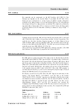
The LCB (ECL00) can be upgraded with the Lock-RS Interface Piggy Board
(Z4P2931) to ECL01. The main differnce is the interface for transfering the
Display-Datas to the computer. The Display-Datas are now being transfererd in
RS232 (or SSI) format and can be processed by any computer fitted with RS232-
Interface. The LCB ECL02 is standardly equiped with the RS232 and SSI-Interfac.
No piggy-board is required for ECL02. The two interfaces can be selected by
jumpers (see chapter ‘Jumper Setting’).

Upgrade to ECL01

10.2

The following components on the mainboard should be exchanged:

1. New Frontpanel (Z12284)

2. R44 must be exchanged with a 680 ohm resistor (20734)

The following signals have to be connected with the main board:

1. TP1 (X5V) -> TP1 Mainboard

2. TP2 (XGND) -> JU7 Mainboard

3. TP3 (RXD) -> J2 9A Mainboard

4. TP4 (TXD) -> J2 9B Mainboard

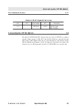
5. Connnect flat-band-cable (9 pol) with the Sub-D-Connector on the front panel

Exchange BSMS-Label with BSMS ECL01-Label

Summary of Contents for DAEDALUS

Page 1: ...BRUKER BRUKER SPECTROSPIN AG SERVICE MANUAL DAEDALUS LOCK Version BSMS 004 ...

Page 2: ...peration of the instrument Unauthorised reproduction of manual contents without written permis sion from the publishers or translation into another language either in full or in part is forbidden This Manual was written by C Gosteli B Jud A Kuster A Schwilch S Leemann C Schumacher Translated and Desktop Published by Craig M Brumby and Beat Jud Spectrospin AG CH 8117 Fällanden Nov 1993 Spectrospin ...

Page 3: ... Lock Hold Operation 28 4 19F Lock Option 31 4 1 Introduction 31 4 2 19F Option Installation 31 4 3 19F Wiring 34 4 4 19F Operation 35 5 Lock Transmitter 37 5 1 Function Description 38 General 38 Digitalization of the 10 MHz Reference 39 60 MHz Multiplier for DDS Clock Frequency 39 N x 10 MHz Multiplier 40 Direct Digital Synthesizer DDS 40 Quadrature Mixer 41 Temperature Unit Modulation 41 Attenua...

Page 4: ...ral 64 Microcontroller 64 Address Decoder in the Lock System 65 VME Interface 66 Reset and Power up Logic 66 RCP Interface 67 DSP Host Interface 67 DSP Section Hardware 67 DSP Section Software 68 Display Data 68 Current Source 69 Serial Interface in the Locksystem 70 Lock Software 72 9 2 Jumper Setting 73 9 3 Print Hardware Version 74 10 Lock RS232 Piggy Board 75 10 1 General 75 10 2 Upgrade to EC...

Page 5: ...ol 87 15 Lock Error Messages 93 15 1 Error Descriptions 93 A Appendix 103 A 1 Technical Data for the H0 Coil 103 A 2 Regulating Range 103 A 3 Frequency Generation 104 A 4 Chemical Shifts 106 A 5 List of Current Bruker NMR Instruments 107 A 6 List of Abbreviations Used 107 B List of Figures 109 C List of Tables 111 D Schematics 113 ...

Page 6: ...Contents 6 Spectrospin AG Daedalus Lock Manual ...

Page 7: ...sition 56 Acquisition Parameters 35 Active Bandpassfilter 56 ADC diagnostic 90 AGC Amplifiers 41 applications software 93 ASX 93 Attenuator 60 Auto Gain 21 Auto Lock 21 Auto Phase 21 Auto Power 21 Autolock 22 91 Autolock H0 Calibration 91 Autolock Mode 88 B Baudrate 69 beep buzzer 26 Blackman Window 11 43 82 Bloch 11 Boot EPROM 93 BSMS Keyboard 21 BSMS Servicetool 34 Buffer Amplifier 60 C Cables 1...

Page 8: ...velopment and debug tools 91 Diagnostic 90 difference experiments 24 Digital Analog Converter DAC 38 Digital Lock Settings 15 Digital Synthesizer 15 Direct Digital Synthesizer DDS 38 40 Dispersion 56 Display 22 Display Cable 17 Display Data 68 Display jumpers 73 Display Mode 21 28 Display mode 89 Display Scaler Board 17 dividers 52 DownLoad 87 DP_RAMError 93 Drift 11 DSP 67 68 DSP Host Interface 6...

Page 9: ... 146 94 Error 148 94 Error 149 95 Error 150 96 Error 151 97 Error 152 97 Error 153 99 Error 155 97 Error 156 96 Error 157 95 Error 158 99 Error 160 99 Error 161 99 Error 162 96 Error 163 98 Error 164 98 Error 165 93 Error 22 98 Error 3 99 Error 30 95 Error 4 95 Error 51 95 Error 52 95 Error 53 96 Error 8 99 Error Code 94 Error Code 12 100 Error Code 31 99 Error Code 32 100 Error Code 33 100 Error ...

Page 10: ... H H0 Power Source 15 H0_CURRENT 91 Hardware Version 74 HF Amplifier 55 HF Bandpass Filter 55 HF Parameters 70 HF Power Supply Failure 95 Highpass Filter 60 hold off 29 hold on 29 Hold Operation 28 Homospoil 91 Homospoil interface 88 HPPR 17 HPPR 19F Selective module 31 HWTesterIsOff 95 HWTesterIsOn 95 I ii 35 imaginary part 89 Init 87 Interface Function 88 J Jumper 68 Jumper Setting 70 73 K Keybo...

Page 11: ...ass Filter 60 M Magnet Type 88 Manual Lock In 27 Manual Lock In 22 Menu Tree 27 Mixer 60 Mode Register 90 ModeBusError 95 MX 89 MY 89 N NMR Control Word 28 No Communication with DSP 95 No FFA Amplifier Signal 96 No FFASignal Found 96 No H0 Coilcurrent 96 No Option 96 No Quadmixer Signal 97 No RFOut Signal 97 No T2H DDSSignal 97 No Z0_Compensation on LCB 98 noise modulation 24 normal lock mode 90 N...

Page 12: ... filtered 89 Rec Blanking On Off 88 Receiver 15 31 59 81 Receiver AGC Voltage Diagnostic 90 Receiver Blanking 44 Receiver Cable 17 receiver gain overflow 24 Reference Signal 38 Regulator Gain 21 Regulator Output 21 22 regulator output 28 Regulator Time Constant 21 reset 87 Reset and Power up Logic 66 RP1 90 RS Baudrate 69 RS232 68 69 RS232 Piggy Board 75 RS Baudrate 22 RX AGC Voltage Failure 99 RX...

Page 13: ...s Blanking On Off 88 Transmitter 15 31 59 82 Transmitter Blanking 44 Transmitter Cable 17 Transmitter HFSection Diagnostic 90 Transmitter Power Range 42 Transmitter Subsections 38 TX_BLNK Off 90 U Upgrade to ECL01 75 UXNMR 35 V Variable Lock Parameters 21 Version 87 VME Interface 15 64 66 W wide bore 88 wiggles 22 23 Wrong AppSW 100 Wrong Datacount 99 Wrongaddress 100 WrongCheckSum 100 WrongRecord...

Page 14: ...8 Spectrospin AG Daedalus Lock Manual ...

Page 15: ...me soaring philos ophy and thorough preparation our Daedalus Lock will perform for you to achieve the ever more exacting demands for NMR in the 90 s Your Manual Contains Your manual features three major areas to help you quickly locate your subject of interest The first two chapters General Description and Operation provide an overview of the entire system with specifics for operation The followin...

Page 16: ...10 Spectrospin AG Daedalus Lock Manual ...

Page 17: ... where Deuterium is the substance of interest an alternative lock channel can be used This alternative channel option uses Fluorine as the lock sub stance The Daedalus Lock is applied to ARX AMX DRX DMX DPX Spectrometers Features 2 2 ULTRA LOW NOISE DESIGN SIGNIFICANT IMPROVEMENTS IN SHORT AND LONG TIME STABILITY LOWEST T1 NOISE IN 2D SPECTRAS INDEPENDEND IN TEMPERATURE CHANGES HIGH SUPPRESSION OF...

Page 18: ... Receiver Fluorine Lock 19F Chemical Shifts 2H Chemical Shifts 19F RX Option 19F TX Option Auto Gain Auto Lock Auto Phase Auto Power BSMS Servicetool Current Source Deuterium Frequency Drift FFA H0 Lock Gain Lock Phase Lock Power Lock Shift Lock Transmitter Lock Hold PLL RS232 Piggy Board Sweep Wiggles Z0_Compensation ...

Page 19: ...Daedalus Lock Catchwords for Bash Daedalus Lock Manual Spectrospin AG 13 Figure 1 Lock Function Diagram ...

Page 20: ...General Description 14 Spectrospin AG Daedalus Lock Manual Mixer BP H0 Coil Probe BP Mixer Rectifier Transmitter ux uy DHreg wm 2 wm 2 LO 0û LO 90 Rectifier Digital Signal Processing Digital Regulator ...

Page 21: ...the Lock Gain setting The IF Signals Dispersion Absorption are digitized in the Receiver and are serial ly forwarded to the Controller Board via optocouplers The sampling rate proceeds at 13 3 kHz per channel There are some other diagnostic signals which are digitized with the same A D Converter for diagnostic purposes The Controller Board receives all User or X32 commands via the VME Interface Th...

Page 22: ...the Lock A D HF NF Control Unit DDS HF Pulse Section D A DSP 56000 uP 80535 VME Interface VME Bus HPPR Probe TX BLNK RCP RX BLNK RCP 2H LO 2H TR TP F0 2H REC 10MHz Serial Bus Power Gain Phase Shift Mode H0 Coil GT01 X32 Lock Display CPU Keyboard X32 Receiver Transmitter Controller Pulse ...

Page 23: ...002745 for 250 MHz Instrument Z002728 for 300 MHz Instrument Z002729 for 360 MHz Instrument Z002730 for 400 MHz Instrument Z002731 for 500 MHz Instrument Z002732 for 600 MHz Instrument Z002736 for 750 MHz Instrument Lock Controller LCB Z002720 for all instruments These three units are built into the BSMS Rack Cables Lock Display Scaler Board GX01 on the GT01 Board X32 H2528 HPPR The Digital Lock i...

Page 24: ...LNK J9 19F TR J6 19F LO J5 2H TR J4 2H LO J3 10MHz 2H_REC J2 2H_LO J3 19F LO J5 LOC REC OUT TRANSM 2H Module TRANDM 19F MOdule 10MHz R L HOLD J4 L Display 1 J3 2 J3 3 J3 5 J3 yellow brown white green LO Upgrade from T 2H Bourndy Preamp Probe Periph F Plug F PFP Bourndy Plug L 9 11 12 10 Z12115 Z1740 Option BSN 18 to BSMS Upgrade from BSN 18 to BSMS ...

Page 25: ...0MHz 2H REC 2H TR TP F0 Upgrade from BSN18 to BSMS PFP Burndy Plug L Preamp Probe Periph Plug F Upgrade from BSN18 to BSMS T 2H Burndy Plug f SE451 10MHz R Z12257 Z2743 Z12256 Z1740 To GT01 GX01 Cable Z12115 L Display Lock Display Console Wiring Z12206 Z12207 Console Wiring To CPU 4 RS232 Interface Cable Z12321 ...

Page 26: ...General Description 20 Spectrospin AG Daedalus Lock Manual ...

Page 27: ...nsmitter cw 60 0 0dBm Output power of the Transmitter cw ECL01 or later LOCK RF GAIN 75 0 155 0 dB Receiver and Pramplifier RF Gain AUTO GAIN LOCK RF GAIN AUTO POWER LOCK POWER AUTO PHASE LOCK PHASE LOCK Previous Set AUTO LOCK FIELD or SHIFT LOCK SHIFT 200 000 200 000 ppm 1H Frequency LOCK DRIFT Field Units per Day only active in lock off and sweep off mode Lock Menu 2 2 1 LOOP GAIN 80 0 dB PI Reg...

Page 28: ...locking on a solvent when the correct field value is not known is to search for the lock signal One approach to finding the lock signal is to set the sweep amplitude to the maximum 100 increase the lock power e g to 0 dBm and increase the lock gain e g to 120 dB The lock DC should be set to ap proximately 75 and the sweep rate to 0 2 Hz Adjust the field value until the lock signal is approximately...

Page 29: ...uced This second regulator uses the parameters described below set from the BSMS keyboard or computer Once lock in is achieved the overall lock results can be improved by adjusting the lock phase to produce the maximum signal amplitude Optimal Operation with the Digital Lock 3 3 One advantage of the digital lock system provided by the BSMS is that the user is no longer restricted to adjusting the ...

Page 30: ...k gain Finally the regulator should be optimized using loop gain and loop time see Lock Parameters on page 21 A large i e less negative loop gain value enables a better field disturbance compensation which is what is desired However if the signal to noise ratio of the lock signal is not sufficient too high a loop gain causes the H0 field to be noise modulated When this occurs the lock line oscilla...

Page 31: ... DRIFT to provide the correct compensation it is necessary to calibrate the mag netic field drift as follows 1 Set the drift to zero 2nd DRIFT and choose 0 with the control knob 2 Insert a sample with a strong lock signal Lock settings with a very high loop gain and good signal to noise ratio AMX600 Lock Power 30 dBm Saturation Lock Gain 90 dB Loop Gain 10 dB Loop Time 0 004 s 2mMol Lysozyme in 90...

Page 32: ... set this parameter to the value found in step 8 with the same polarity This completes the drift adjustment and further cor rections are usually not necessary 10 To save the drift value first select the menu on the keyboard 2nd and Y3 11 Enter the security code 4 Service ENTER 4 1 Sec Code ENTER en ter the code with control knob and ENTER a beep sounds if the code is cor rect ESC and you are now i...

Page 33: ...eld 2 2 Loop Filter requires Password 2 7 RS Baudrate requires Password 300Baud 0 600Baud 1 1200Baud 2 2400Baud 3 4800Baud 4 9600Baud 5 19 2KB 6 default 38 4KB 7 disable 0 enable 1 Field 0 Shift 1 Re 0 RE LP 1 Im 2 Cont out 3 Re ex 4 Re Lp ex 5 FFA Spec 6 Cont ex 7 DIAGLoLi 8 DIAG sin 9 DIAG cos 10 DIAGCoEx 11 DIAG 1 12 DIAG2 13 DIAG3 14 2 8 Lockin PStep requires Password ...

Page 34: ...Connector N3 N as the Lock Hold Program the hold pulse if possible according to the following diagram It is not rec ommended to lock in between the end of the gradient and the start of the acquisi tion even there is enough time Caution There is a short Lock in Spike ca 100ms at the Regulator output after going down of the hold pulse Be sure that the acquisition starts after or ends before this spi...

Page 35: ...ospin AG 29 Example of a Lock Hold Pulse Program xxx setf2_3 january 1993 program to control NMRCONTROL F2 3 written based on UXNMR 921218 on ARX500 1 ze 2 d30 setf2 3 lock hold on 3 d31 setf2 3 lock hold off 6 go 2 7 exit e g d30 10ms e g d31 20ms ...

Page 36: ...Operation 30 Spectrospin AG Daedalus Lock Manual ...

Page 37: ...orine Lock Option BSMS BSMS L RX Option 19F Z002748 for all instruments BSMS L TX Option 19F Z002749 for 200 MHz Instrument BSMS L TX Option 19F Z002750 for 250 MHz Instrument BSMS L TX Option 19F Z002751 for 300 MHz Instrument BSMS L TX Option 19F Z002752 for 360 MHz Instrument BSMS L TX Option 19F Z002753 for 400 MHz Instrument BSMS L TX Option 19F Z002754 for 500 MHz Instrument BSMS L TX Option...

Page 38: ...9F board e g 19F_LO and 19F_TR are con nected to the front panel of the Lock Transmitter L TX case via coaxial cables with SMA connectors Before screw on the SMA connector the front foil has to be pierced through at the corresponding point with a sharp object The 19F_LO signal to the L RX Option 19F board has to be connected in the same way Figure 5 L TX Option 19F Installation 1 Back Side BSMS L ...

Page 39: ...19F Option Installation Daedalus Lock Manual Spectrospin AG 33 Figure 6 L RX Option 19F Installation Back Side BSMS L RX Option 19F L RX Mainboard 19F LO ...

Page 40: ... B board functions LCB 4 Version Config 2H 19F 1H Probehead BSMS BSMS L TX L RX LCB BSMS 19F LO 19F LO 19F TR 2H LO 2H LO 10MHz 2H REC 2H TR TP F0 Upgrade from BSN18 to BSMS PFP Burndy Plug L Preamp Probe Periph Plug F Upgrade from BSN18 to BSMS T 2H Burndy Plug f SE451 10MHz R Z12257 Z12257 Z2743 Z12256 Z1740 To GT01 GX01 Cable Z12115 L Display Lock Display Console Wiring Z12206 Z12207 Console Wi...

Page 41: ...bility to assert the 19F mode in the BSMS Execute the fol lowing commands with the BSMS Servicetool bsms B board functions LCB B 5 Lock Substance 5 Read or Write Lock Substance R W w Select Lock Substance 0 Deuterium 1 Option Enter Value 1 After these steps the BSMS Servicetool can be exited The 2H mode could be acti vated in the same manner by selecting 0 Deuterium as the lock substance The 19F s...

Page 42: ...regulating characteristic in 19F mode is also different from 2H mode After re ducing the Loop Gain by 15dB regulating characteristic will correspond with the 2H mode Lock Settings for 19F which correspond with the old Analog Lock Loop Gain 47dB Loop Time 0 136s ...

Page 43: ...Bus 12 Bit 8Bit SHAPE0 6 COUNT0 10 PL_CLK ADC_CONV RP1 RP2 CH_SEL0 2 FFA to Receiver Amp TP_F0 to HPPR TP DDS PHASE_LOAD1 2 CS_CNTR CS_PWR CS1_DDS CS2_DDS CS_GAIN CS_PLL CS1_DDS CS2_DDS CS_PWR P_BNK0 3 Mixer Amp Amp λ 4 BP BP PLL Mixer BP Amp Amp Quad F_TEMP LCB 2H_TR 2H_LO X_TR X_LO 10MHZ RCP RCP X OPTION D_10MHZ 60MHZ N 10MHZ L_SUBST UAGC J5 J6 J3 J4 J9 J8 J2 FFA J7 from to LCB I 2 C I2C Bus EPR...

Page 44: ...ped with a Deuterium Lock The Transmitter is mounted on one four layer board Z4P2866 and contains the following subsections Schematics Z4S5381 2 of 10 Digitization of the 10 MHz Reference 60MHz Multiplier N x 10 MHz Multiplier Depends on Instrument Schema Z4S5381 3 of 10 Direct Digital Synthesizer DDS Schema Z4S5381 4 of 10 Quadrature Mixer Modulator for Temperature Unit Attenuator and Switching S...

Page 45: ... between zero and five volts because of charging at C61 60 MHz Multiplier for DDS Clock Frequency 5 1 3 Using the different time delays from two gates Pins 4 and 5 of IC81 a needle im pulse Pin 6 is generated from the digitized 10 MHz square wave signal Such a needle impulse contains all multiples of 10 MHz 10 20 30 MHz The R107 re sistor and the C60 condensor determine the pulse width of the need...

Page 46: ... make variations in the lock frequency Lockshift possible The DDS module IC6 calculates with a clock rate of 60 MHz the amplitude values for the desired output frequency The frequency is dependent upon the operating frequency and lies between 9 and 16 MHz The small est frequency shift is 14 mHz The DDS also allows you to quickly switch the output signal phase This is impor tant because the transmi...

Page 47: ...d by trimming the two condenser C174 and C175 The mixer product Deuterium frequency is given to the LO Output via the M3 am plifier and the following attenuator In addition the LO Signal is rectified and as a DC voltage used for diagnostics via the DIAG_3 connection Temperature Unit Modulation 5 1 7 According the prnciple described in Patent P4947 stabilizing the temperature of an NMR probe requir...

Page 48: ...livers the control signal UAGC This is possible because the control voltage UAGC acts in a linear fashion upon the transmitter power The Zener Diode limits the UAGC to a maximum of 12 V PFP FFA Mode Switching 5 1 10 The transmitter signal from the AGC amplifier is divided after the amplifier MOD1 One part is used for the X Option e g 19F the other part is amplified again in MOD2 In normal lock ope...

Page 49: ...the P_BNK0 3 connections and optocouplers IC16 IC17 IC18 An 11 Bit counter counts the addresses from 0 to 2K A0 to A10 The 1MHz counter clock is generat ed by dividing the 10 MHz reference IC30 Using the RCP pulses RX_BLNK and TX_BLNK the receiver and transmitter are switched out in normal lock mode PFP The two signals are galvanically separated from the lock electronics by an optocoupler IC15 The...

Page 50: ...ted from the Lock electronics by an optocoupler TX_BLNK Transmitter Blanking as above CONT_DATA Serial Data from the Controller CONT_WR Write Signal for the Serial Bus CONT_CLK Clock for the Serial Bus CONT_A0 2 Addresses for the Serial Buses that are decoded in IC23 0 Status Shift Register 1 Lock Power 2 DDS 3 DDS 4 Lock Gain 5 PLL for Option CONT_DATAR Connection to read back the serial data for...

Page 51: ...00us 300us 0us 100us 200us 300us 0us 100us 200us 300us 0us 100us 200us 300us 0us 100us 200us 300us 0us 100us 200us 300us 0us 100us 200us 300us 0us 100us 200us 300us 0us TP RP1 RP2 PHASE_LOAD2 PHASE_LOAD1 ADC_CONV CH_SEL0 CH_SEL1 CH_SEL2 NF 3 33kHz 40 150 190 300 45 148 195 298 41 42 191 192 149 150 299 300 9 10 34 35 59 60 5 30 80 105 30 55 105 130 25 26 50 51 0 Deg ...

Page 52: ...V as in PFP mode 6 DDS Diag 12k FF 0 2047 0 ADC_CONV PHASE_LOAD2 as in PFP mode 7 SSB M Diag 14k FF 0 2047 0 ADC_CONV as in PFP mode 8 TX HF Diag 16k 00 0 2047 0 ADC_CONV as in PFP mode 9 TX PA Diag 18k Square Wave 0 2047 0 ADC_CONV u TP period 10 LO RX Diag 20k FF 0 2047 0 ADC_CONV as in PFP mode 11 RX Diag Ch1 22k FF 0 2047 0 ADC_CONV as in PFP mode 12 RX Diag Ch2 24k FF 0 2047 0 ADC_CONV as in ...

Page 53: ...Spectrospin AG 47 Figure 9 Pulse diagram FFA 1 since pre FFA active FFA TP RP1 RP2 PHASE_LOAD1 PHASE_LOAD2 NF ADC_CONV CH_SEL0 CH_SEL1 CH_SEL2 0us 0us 0us 0us 0us 0us 0us 0us 0us 0us 0us 250 255 383us 2k Pulse T 250us T 125us 508us 260us 261us ...

Page 54: ...ag 1 1 0 0 0 0 1 1 0 5 AD Bus Diag 1 1 0 0 0 0 0 0 0 6 DDS Diag 1 1 0 0 0 0 0 1 0 7 SSB M Diag 1 1 0 0 0 1 0 1 0 8 TX HF Diag 1 1 1 0 0 1 1 0 0 9 TX PA Diag 1 1 E 0 0 1 1 0 1 10 LO RX Diag 1 1 0 1 0 1 1 1 0 11 RX Diag Ch1 1 1 0 1 0 0 0 0 0 12 RX Diag Ch2 1 1 0 1 0 1 0 0 0 13 RX TX Diag C 299 1 1 E E E E 0 0 Remarks E The signal in question comes from the EPROM C Condition and value of the Counter ...

Page 55: ...ware Version 5 1 13 Tabelle 6 L TX Print Version R86 R84 R85 Print Number ECL Description Changes 10K 330 Z4P2866A Prototype with out diagnostic milled housing 10K 680 Z4P2866B ECL00 moulded housing 10K 1K Z4P2866C ECL01 10 db less Power no Transpiggy necessary I2 C EPROM ...

Page 56: ...Lock Transmitter 50 Spectrospin AG Daedalus Lock Manual ...

Page 57: ...ro vides the local oscillator signal for the inverse mixing process on the 19F RX Op tion board where the Fluorine frequency is shifted back to Deuterium in order to use the normal Deuterium lock receiver path 19F TX Option Block Diagram 6 1 2 The block diagram of the lock transmitter gives information about the environment of the 19F TX Option see the lock transmitter section in this manual A det...

Page 58: ... mixer output so that the following amplifier stages are not driven into saturation The filter also provides impedance matching of the mixer output to the input of the following amplifier After a first amplifier stage a lowpass filter suppresses harmonics of the local oscillator signal and unwanted mixing prod ucts above the 19F frequency A second amplifier stage provides enough power at the 19F_T...

Page 59: ...3kHz fo 1kHz 30dB Range 14Bit ADC Phaseshifter Active Active GaAs Switch Options X_LO 1 1 2 2 Pos1 RP1 RP2 L_SUBST 1 2 1 2 Pos1 FFA 0 Pos2 FFA 1 Pos1 FFA 0 Pos2 FFA 1 Pos1 FFA 0 Pos2 FFA 1 Pos1 FFA 0 Pos2 FFA 1 1 1 2 2 Pos2 RP1 RP2 L_SUBST POWER_CONT UAGC FIELD_SENS DIAG_1 DIAG_2 DIAG_3 Mx CH1 My CH2 f 2H 1MHz f X f LO f 2H f 2H f 2H 3 33kHz f 2H FFA f 2H f 2H 3 33kHz f 2H FFA SCK SRD FSR RP1_C to...

Page 60: ...nsmitter This results due to the phase switching receiver in an audio frequency of 3 3 kHz The resulting signal is once again amplified filtered and digitized in the low frequency section At the Receiver input the Lock signal is between 75 and 15dBm The variable gain amplifiers in the HF and LF sections compensate the different in put levels The output amplitude is then optimized for the best A D ...

Page 61: ...very little phase shifting Two cascaded AGC amplifiers SL 6140 from Plessy with a phase shift of just 20 de grees 100 MHz meet this requirement ably Its surface mount design allows a good high frequency layout with short conducting paths HF Bandpass A fourth order Bessel Bandpass with fo Deuterium frequency suppresses dis turbing signals from the following mixer The filter is optimized to a minimu...

Page 62: ...Instruments Acquisition 7 1 4 An A D converter digitizes the absorption and dispersion lock signals alternately and send these serially via the Optocoupler galvanic isolation to the Lock Control ler Board for further processing A DSP101 from Burr Brown is used as A D converter This is a single channel SAR converter ENOB 14Bit The SAR converter has the advantage that it is very exact around zero Si...

Page 63: ... Version 7 1 5 Tabelle 7 L RX Print Version R114 R115 R116 Print Number ECL Description 10K 0 Z3P2853B Prototype without diagnostic milled hous ing 10K 330 Z3P2853C ECL00 moulded housing 10K 680 Z3P2853D E ECL01 new mixer TDA6130X4 improved leakage and production performance ...

Page 64: ...Lock Receiver 58 Spectrospin AG Daedalus Lock Manual ...

Page 65: ...y range in the receiver option The same connection X_REC from the preamp to the receiver is used for the 19F Signal as for the 2H signal We therefore require switching to the option at the input and output Figure 13 Signal path in Receiver with built in Option Trouble free upgrades to optional lock are available on site Upgrading to Fluorine requires alterations to the transmitter as well as the r...

Page 66: ...ow frequen cy interference A 10 MHz signal is suppressed by more than 30 dB The cutoff fre quency is 30 MHz f2H 200MHz Buffer Amplifier The buffer amplifier decouples both the high and low pass filter and compensates the mixer filter and attenuator losses The unit employed is a MSA 0186 from Avantek Its operating resistance is 560 Ohm The DC working value of the MSA 0186 is chosen such that the DC...

Page 67: ...oltage supply LOCK_P15V and LOCK_AGND are connected by print plugs The X_REC signals and X_IF are connected directly to the Receiver board with the SMB print connectors The X_LO signal is connected to the front of the Receiver case on a SMA plug and sent to the X_OPTION RX via a coaxial cable Tabelle 8 19F RX Option Print Version R10 R11 Print Number ECL Description 330 Z4P2908A ECL00 19F RX Optin...

Page 68: ...19F RX Option 62 Spectrospin AG Daedalus Lock Manual ...

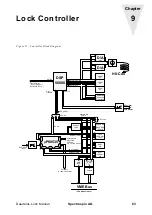
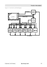
Page 69: ...0 EPROM 128k EPROM 32k Address Latch Dual Port RAM 1k Latches VME Logic Serial Bus to from Transmitter Analog Inputs Diagnostic Data Bus 8Bit up Control Bus 16 Bit D A X RAM 2k Y RAM 2k P RAM ADDRESS DECODER Data Bus 8Bit TIPAL20L8 16 Bit 16 Bit Data Bus 24 Bit Control Bus 4k SSI TX SSI RX from Receiver Host Interface A0 A3 Address Bus Adress Bus 16 Bit Real Imag Part D0 D8 DSP_HREQ PR Code RX TX ...

Page 70: ...128K 8 Flash EPROM and an EP910 as Addressdecoder The EPROM contains the Startup and Download software Applications software is stored in the Flash EPROM The 80C535 Bus structure consists of a 8 Bit Databus a 16 Bit address Bus and 5 control connections In the beginning of a Fetch Execute sequence the addresslatch IC37 latches the addresses A0 A7 with the signal ALE Port 0 is now changed to functi...

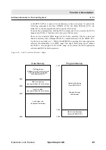
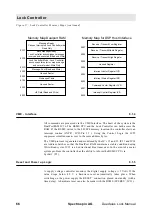
Page 71: ...M for communication with the BSMS CPU On the lock controller is a 1 MByte FlashEPROM containing the lock application software downloadable in its ROM range The upper Flash range from Address 0x10000 is also mapped in the RAM range and contains the DSP application software and DSP default parameters Figure 16 Lock Controller Memory Maps Data Memory DSP Application Software X and Y memory stored in ...

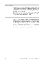
Page 72: ...Logic 9 1 5 A supply voltage controller monitors the digital supply voltage 5 Volt If the value drops below 4 5 V a hardware reset automatically takes place When switching on the power supply the RESET connection placed on standby with a time delay A hardware reset can also be made with the BSMS SYSRES IC31 83FF 83FE 83FD 8300 8200 8100 8302 8000 Memory Map Dualport RAM Message Ready Causes Interr...

Page 73: ... Hardware 9 1 8 The DSP operates in Bootstrap mode The mode is read in after the Reset with the Pins MODA and MODB The DSP connection D23 is grounded with a 10k Resistor This leads to the internal Bootstrap Program being activated in DSP after a Reset and the program being loaded via the Host Interface The data from the Receiver Dispersion Absorption and external Field sensor signals are read into...

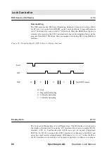
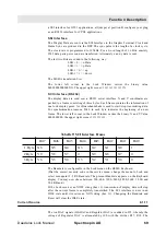
Page 74: ... the DSP Host Interface Figure 18 Downloading the DSP Software Timing diagram Display Data 9 1 10 The Lock sends Display data in two different ways The SSI interface which serves the Graphic Terminal GT01 and the SCI Interface which serves a normal RS232 interface CPU 4 Lockboards with ECL00 must get an upgrad Piggyboard Z4P2931 to ECL01 to support the RS232 Interface Lockboards with ECL02 and new...

Page 75: ...t A softwarehandshake is used to start stop transmitting data For synchronization reasons Bit 0 in each byte indicates the beginning of a new frame The lower left corner in the Lock Window carries the binary X and Y Value 0000000000 the upper right corner 1111111111 The Baudrate is configurable in the Lockmenu on the BSMS Keyboard Dial the correct security code in the service menu change the menu ...

Page 76: ...1 mA The Regulator DAC has a range of 1 69 mA Serial Interface in the Locksystem 9 1 12 You can set various HF Parameters via the lock controller serial interface These are transmitter power DDS frequency DDS phase lock systems mode and receiver gain The serial interface operates as a synchronized data transfer The various devices are selected by four adddress connections They are address decoded ...

Page 77: ...spin AG 71 Figure 19 Serial Lock Control Bus Diagram MUX D A Port 1 Port 2 Port 0 Port 3 Port 4 Port 5 µP 80535 Port 6 D A DDS Freq DDS Phase Mode Reg Gain Power Address Bus Device Select Data Return Data Return Data Control Bus Option Address DECODER ...

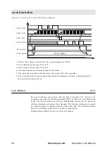
Page 78: ...khold interupt has its own interrupt routine because of time considerations Software Design details are not covered in this manual CONT_DATA CONT_CLK CONT_WR CONT_DATAR CONT_ADDR Device Address Device Select 1 2 3 4 5 1 LCB sets Device Address on Port 5 Pin 0 Pin3 causes Chipselect on L2H IC23 2 Data is clocked by positive edge of Cont_CLK 3 Data is strobed by positive edge of Cont_WR 4 LCB clocks...

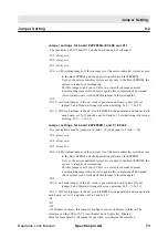
Page 79: ... mind wrong silk screen printing Ju 9 Ju 11 Jumper settings for board Z4P2859B and C ECL02 Two inscriptions used for jumpers Ju and J Ju is not equal to J Ju4 J4 JU3 always on JU4 always on JU5 always on JU6 on Download jumper if this jumper is set the microcontroller system access to the Boot EPROM and the application software Flash EPROM Not set the microcontroller system access only to the Boot...

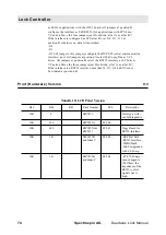
Page 80: ... as SCI driver All jumpers at position B select the RS232 interface as SCI driver Caution Move the three jumpers just blockwide all at A or all at B If the interface is a RS232 interface note that J4 J13 J14 and J15 must be situated at position B Print Hardware Version 9 3 Tabelle 10 LCB Print Version R43 R44 R45 Print Number ECL Description 10K 0 Z4P2859 Prototype with out H0 diagnostic 10K 330 Z...

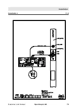
Page 81: ...s standardly equiped with the RS232 and SSI Interfac No piggy board is required for ECL02 The two interfaces can be selected by jumpers see chapter Jumper Setting Upgrade to ECL01 10 2 The following components on the mainboard should be exchanged 1 New Frontpanel Z12284 2 R44 must be exchanged with a 680 ohm resistor 20734 The following signals have to be connected with the main board 1 TP1 X5V TP...

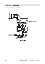
Page 82: ...Lock RS232 Piggy Board 76 Spectrospin AG Daedalus Lock Manual Figure 21 Connections with the Mainboard Connect with J2 9B Connect with J2 9A Connect with TP1 Connect with JU7 ...

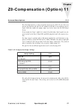
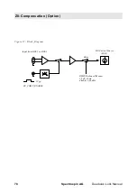
Page 83: ...he input stage is realized with a differential amplifier for well disturbances sup pression With an external RCP Pulse Z0_COMP_ENABLE the analog signal path can be switched to the current source with a fast analog switch IC4 If no external pulse is available the switch has to be closed by setting jumper JU1 The gain for the two different applications can be set with jumper JU2 Table 11 Z0 Compensa...

Page 84: ...Compensation Option 78 Spectrospin AG Daedalus Lock Manual Figure 22 Block_Diagram Input from BGU1 or BGU2 Z0_COMP_ENABLE 1Vpp BSMS Keyboard Menue 2 5 Z0 Comp disable or enable H0 Current Source LCB Relay ...

Page 85: ...Installation Daedalus Lock Manual Spectrospin AG 79 Installation 11 2 ...

Page 86: ...Z0 Compensation Option 80 Spectrospin AG Daedalus Lock Manual ...

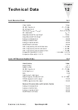
Page 87: ...23 dBm 1dB Compression point at medium Gain 42 dBm 1dB Compression point at maximum Gain 75 dBm Temperature Gain drift 15 450 C 0 12 dB K 1 4 K Temperature Phase drift 15 450 C 0 5 o K Lock 19F Receiver Option Data 12 2 Characteristics Values Supply Voltage 15 V Supply Current 20 mA 2H_REC Input Level 15 75 dBm X_LO Input Level 7dBm Gain 0 dB VSWR at the X_REC Input 2 Output Frequency Passband at ...

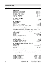
Page 88: ...ut J4 Pulse at Lock Mode PFP Output Frequency f2H Pulse Shape Type Blackman Window Pulse Level 50 10 dBm Pulse Level L TX ECL01 or higher 60 0 dBm Pulsewidth at half height 13 16 µs Entire pulsewidth at the base 32 37 µs Repetition Frequency 6 66 kHz Transmitter Out Pulse Leakage Level 75 dBm Temperature Level Drift 15 45o C 1 per K 2H_TR Output J4 Pulse at Fourier Mode FFA Output Frequency f2H Pu...

Page 89: ...t Current 150 190 mA Transmitter Characteristics with built in Option 19F LO Output Output Frequency see Appendix fLO Output Level 7 0 dBm 19F TR Output Output Frequency see Appendix f19F Output Level f19F 60 0 dBm Spurious near f2H Lock Power 0 dBm 60 dBm Spurious fLO 10 dBm On Off Ratio f19F 100 dB Lock Controller Data 12 5 Current Source Current Range 170mA Current Noise 0 01 10Hz 400nApp Cutof...

Page 90: ...Technical Data 84 Spectrospin AG Daedalus Lock Manual ...

Page 91: ...need two different extension boards for its two 96 Pin connectors The upper one in the BSMS Rack is the VME Bus and request an VME Extension Board multilayer A simple one to one connection is requested at the lower 96 Pin Connector that transmitts the digital control signals You may order these two boards with the necessary installation kit at Rotronic AG Grindelstrasse 6 CH 8303 Bassersdorf Tel 0...

Page 92: ...Trouble Shooting 86 Spectrospin AG Daedalus Lock Manual ...

Page 93: ...l download function may cause an not corresponding software config uration at the BSMS Normally the path for BSMS software is bsmssw Example Enter path and name of file to download bsmssw lock hex An infostring Erasing Flash EPROM indicates that the downloading has begun After the Flash EPROM is erased completely a linecounter shows the current state of the download procedure This counter will rai...

Page 94: ...utolock routines since the magnets have different transfer constants G Amp see table Technical Data for the H0 Coil and H0 Frequency and Regulating Range for more details The Default Value is 0 equal to standard bore Write 1 for wide bore and 2 for super wide bore magnets Trans Blanking On Off 14 0 8 This functions enables disables lock transmitter blanking To blank no transmitter signal the trans...

Page 95: ...ew DDS frequency in Hz Writing a new DDS Frequency O changes the default DDS value and also the frequency variation caused by Lock Shift 1ppm defaultfreq 1E 06 Examples 1 Locked with CFCl3 as lock compound New sample has C6F6 as lock compound Refer to 19F chemical shift table referenced to CFCl3 δ ppm for C6F6 is 163 New Lock Shift is 163ppm W 163000 Example 2 Your 500 Mhz Magnet is 40KHz 2H below...

Page 96: ... on the transmitter See table Pulsbanks and Counters for more de tails It is the hexadecimal value witch is loaded into the status register Remind that the whole lock system depends on this register pulses DSP uso Example Pulses TP RP1 RP2 uso like the transmitter HF section diagnostic L_SUBST High TX_BLNK Off RX_BLNK ON Sheet Transmitter Pulse_Section shows the status register P_BNK0 P_BNK3 selec...

Page 97: ...tion Autolock H0 Calibration 14 0 19 This selection is not in the LCB menu but in can be found in the following menu 5 BSMS system functions 9 Calibration Procedures 7 Autolock H0 calibration procedure The current source on the LCB is built with analogue components and has therefore a finite accuracy This fact causes sometimes an Autolock failure With an exact ad justment of the current source the...

Page 98: ...BSMS service tool 92 Spectrospin AG Daedalus Lock Manual ...

Page 99: ...is read in again by the microprocessor and compared with the transmitted value If the values are not the same a LOCK DDS Freq Bus Error is generated WR CLK CS1_DDS CS2_DDS DATA LOCK FREQ_RETURN LOCK DDSPhaseBusError Error 132 This is displayed if the DDS Phase could not be loaded The microprocessor on the lock controller board loads the shift register IC7 IC10 in the Lock Transmitter via a serial ...

Page 100: ...HC_10MHZ ADC_CONV LOCK DSP RAM Checksum Error 148 Appears if downloading of the DSP application software was done but the Microcontroller and the DSP calculated different Checksums Possible Causes Failure on the Host Bus some bits missing at the DSP side Parts of the DSP Processor system on the LCB do not work correctly IC18 IC19 IC20 LCB uP A0 A2 uP D0 D7 uP Bus Control Signals DSP whole DSP Proc...

Page 101: ...LOCK_P5V and LOCK_N5V are checked by the Microcontroller The supplies are multiplied by a individual factor and added to a common signal L RX IC18 Possible Causes One or several Supplies missing Some Power Supplies do not fulfil their specifications MUX L RX IC19 Pin 10 LOCK_P15V LOCK_N15V LOCK_P5V LOCK_5V LOCK HWTesterIsOff Error 50 Function is only available in Hardware Testmode LOCK HWTesterIsO...

Page 102: ...tput signal If any other errors appear in addition then attend to them first Diagnostic Channel Pulsbank Nr 9 Signalname DIAG_1 AGC_OUT FFA L_SUBST ADC_CONV TP LOCK No FFASignal Found Error 144 Displayed if no lock signal can be found after activating the Autolock Possible Causes Correct Field is more than 1000 Hz away from the Lock NMR Signal There is no sample in the magnet Incorrect Signal Path...

Page 103: ... DIAG_1 L TX UAGC 2H_LO AGC_OUT FFA 19F_OPT L_SUBST LOCK NotSameBootRoutine Error 39 The lock boots from an EPROM The boot routine stored in this EPROM must correspond to the downloaded application software The download all boards function in the BSMS service tool guarantees software consistency To restart downloading take out jumper 6 reset the BSMS clear the lock errormessage 11 and start downlo...

Page 104: ... generated WR CLK CS_PWR DATA PWR_RETURN LOCK PowerFail Error 13 This error may appear if either a voltage fluctuation was detected on the Lock Controller Board IC5 monitors the 5V VCC supply on the LCB or the LOCK executed a software reset For example after a manual Download Use the Init feature in the BSMS tool to maintain regular lock operation LOCK ProgrammerFail Error 36 Special algorithms al...

Page 105: ... Possible Causes The Pulse Section in the transmitter is not working correctly 10 MHz reference is not connected Failure in Receiver Acquisition Section IC9 Too much noise in Receiver HF Section Too much noise in Receiver NF Section Failure in AGC Control Voltage Unit If the Error Lock RX AGC Voltage Failure appears in addition then attend to it first Diagnostic Channel Pulsbank Nr 5 NF1 NF4 NF_OU...

Page 106: ...ely Your download file is damaged contact your local Bruker service agent for a correct LOCKxx HEX file To restart the download reset the BSMS and clear the LOCK Errormessage 11 The lock uses only the booteprom no valid application software in its program memory LOCK WrongCheckSum Error 34 The lock application software is a INTEL Hex file Every line in this file gets a checksum The lock calculates...

Page 107: ...Error Descriptions Daedalus Lock Manual Spectrospin AG 101 ...

Page 108: ...Lock Error Messages 102 Spectrospin AG Daedalus Lock Manual ...

Page 109: ... 325 27 49 9 140 63 Super Wide Bore previous versions 54 229 91 35 3 107 144 Super Wide Bore new version 53 85 229 27 35 2 126 178 Table 14 H0 Frequency and Regulating Range H0 Coil Type H0 Frequency Range kHz 2D Regulating Range Hz 2D Standard Bore Lock Software lockae hex or later 12 3 122 195 49 Wide Bore previous versions Lock Software lockae hex or later 9 7 96 154 39 WideBore new version Loc...

Page 110: ...olvent the TMS line appears at the exact frequency for instance 500 13000MHz Table 16 New Deuterium Frequencies Table 15 Deuterium Frequencie which correspond with the old Analog Lock Instrument Deuterium Frequency Mixing Frequencies Variation f2H MHz N 10 MHz fDDS MHz MHz 200 30 721754 20 10 721754 0 5 250 38 397193 50 11 602807 0 5 300 46 072632 60 13 927368 1 360 55 283158 70 14 716842 1 400 61...

Page 111: ...0 12 123609 1 750 115 149522 100 15 149522 1 Table 17 Fluorine Frequency Generation Instrument Fluorine Frequency Mixing Frequencies Variation f19F CFCl3 MHz M 1 MHz N 10 MHz fDDS MHz MHz 200 188 310273 158 20 10 310273 0 5 250 235 357261 197 50 11 642739 0 5 300 282 404249 236 60 13 595751 1 360 338 860634 284 70 15 139366 1 400 376 498225 315 50 11 498225 1 500 470 592200 394 90 13 407800 1 600 ...

Page 112: ...enced to TMS Acetic 2 03 Aceton 2 04 CDCL3 7 24 CD2Cl2 5 32 CD3CN 1 93 C6D6 7 28 D2O 4 70 DEE 1 07 DME 3 30 DMF 2 91 DMSO 2 49 Dioxan 3 53 EtOH 1 11 MeOH 3 30 THF 1 73 Tol 2 09 Pyr 8 71 Table 19 Some Representative 19F Chemical Shifts Referenced to CFCl3 Compound Shift ppm Referenced to CFCl3 C6F6 163 F2C CF2 135 CF2Cl2 8 CF2Br2 7 CFBr3 7 4 ...

Page 113: ...og Converter DDS Direct Digital Synthesizer DPR Dual Port RAM DSP Digital Signal Processor ECL Emitter Coupled Logic EPLD Electrical Programmable Llogical Device FFA Fast Field Adjustment HF High Frequency HP High Pass Filter HPPR High Performance Preamplifier Bruker Product Name IF Intermediate Frequency LCB Lock Controller Board LF Low Frequency LO Local Oscillator LP Low Pass Filter L RX Lock R...

Page 114: ...Appendix 108 Spectrospin AG Daedalus Lock Manual ...

Page 115: ... 6 19F TX Option 51 Figure 10 19F TX Option Block Diagram 51 7 Lock Receiver 53 Figure 11 Receiver Block Diagram 53 Figure 12 Block Diagram of Receiver Concept 54 8 19F RX Option 59 Figure 13 Signal path in Receiver with built in Option 59 Figure 14 X_Option Block Diagram 60 9 Lock Controller 63 Figure 15 Controller Block Diagram 63 Figure 16 Lock Controller Memory Maps 65 Figure 17 Lock Controlle...

Page 116: ...dalus Lock Manual 12 Technical Data 81 13 Trouble Shooting 85 14 BSMS service tool 87 Figure 23 Mode Register L TX IC27 90 15 Lock Error Messages 93 A Appendix 103 B List of Figures 109 C List of Tables 111 D Schematics 113 ...

Page 117: ... Table 5 PAL Outputs at the various operating modes 48 6 19F TX Option 51 7 Lock Receiver 53 8 19F RX Option 59 9 Lock Controller 63 10 Lock RS232 Piggy Board 75 11 Z0 Compensation Option 77 Table 11 Z0 Compensation Jumper Settings 77 12 Technical Data 81 13 Trouble Shooting 85 14 BSMS service tool 87 15 Lock Error Messages 93 A Appendix 103 Table 13 Technical Data for the H0 Coil 103 Table 14 H0 ...

Page 118: ...Manual Table 17 Fluorine Frequency Generation 105 Table 18 Some Representative 2H Chemical Shifts 106 Table 19 Some Representative 19F Chemical Shifts Referenced to CFCl3 106 B List of Figures 109 C List of Tables 111 D Schematics 113 ...

Page 119: ...ter component plan Transmitter component list 19F Transmitter Option Index A 19F Option Transmitter schematics 19F Option Transmitter componentplan 19F Option Transmitter component list Lock Receiver Index C Receiver schematics Receiver component plan Receiver component list Lock Receiver Index D and E same schematics Receiver schematics Receiver component plan Receiver component list 19F Receiver...

Page 120: ...iggy Board RS232 Piggy Board schematics RS232 Piggy Board component plan RS232 Piggy Board component list Z0 Compensation Option Z0 Compensation schematics Z0 Compensation component plan Z0 Compensation component list Cables Lock Display Cable RS232 Lock Display Cable for GT01 Lock Test Equipment Index A Test Equipment schematics Test Equipment component plan Test Equipment component list Lock Blo...

Page 121: ... CONT_WR CONT_WR DATA_RETURN RP1 RP2 DGND DGND CONT_A2 CONT_A3 VCC VCC RP1_C RP1_C SCK SCK SRD SRD LOCK_N5V LOCK_N5V LOCK_DGND LOCK_P5V LOCK_P5V LOCK_DGND REC_TYPE REC_TYPE TRANS_TYPE TRANS_TYPE PRCODE_REC PRCODE_TRANS PRCODE_TRANS CONT_DATA CONT_CLK CONT_DATAR CONT_A0 CONT_A1 H0CURR_P H0CURR_N H0_P H0_GND H0_N CLK OPT_REC OPT_REC OPT_TRANS OPT_TRANS PRCODE_REC 1a 8a 16a 1a 8a 16a 32a 24a 1a LCB J...

Page 122: ...116 Spectrospin AG Daedalus Lock Manual ...

Page 123: ...Daedalus Lock Manual Spectrospin AG 117 Lock Transmitter Index B ...

Page 124: ...118 Spectrospin AG Daedalus Lock Manual ...

Page 125: ...Daedalus Lock Manual Spectrospin AG 119 Lock Transmitter Index C ...

Page 126: ...120 Spectrospin AG Daedalus Lock Manual ...

Page 127: ...Daedalus Lock Manual Spectrospin AG 121 19F Transmitter Option Index A ...

Page 128: ...122 Spectrospin AG Daedalus Lock Manual ...

Page 129: ...Daedalus Lock Manual Spectrospin AG 123 Lock Receiver Index C ...

Page 130: ...124 Spectrospin AG Daedalus Lock Manual ...

Page 131: ...Daedalus Lock Manual Spectrospin AG 125 Lock Receiver Index D E ...

Page 132: ...126 Spectrospin AG Daedalus Lock Manual ...

Page 133: ...Daedalus Lock Manual Spectrospin AG 127 19F Receiver Option Index A ...

Page 134: ...128 Spectrospin AG Daedalus Lock Manual ...

Page 135: ...Daedalus Lock Manual Spectrospin AG 129 Lock Controller Index A ...

Page 136: ...130 Spectrospin AG Daedalus Lock Manual ...

Page 137: ...Daedalus Lock Manual Spectrospin AG 131 Lock Controller Index B C ...

Page 138: ...132 Spectrospin AG Daedalus Lock Manual ...

Page 139: ...Daedalus Lock Manual Spectrospin AG 133 Lock RS232 Biggy Board ...

Page 140: ...134 Spectrospin AG Daedalus Lock Manual ...

Page 141: ...Daedalus Lock Manual Spectrospin AG 135 Z0 Compensation Option ...

Page 142: ...136 Spectrospin AG Daedalus Lock Manual ...

Page 143: ...Daedalus Lock Manual Spectrospin AG 137 Cables ...

Page 144: ...138 Spectrospin AG Daedalus Lock Manual ...

Page 145: ...Daedalus Lock Manual Spectrospin AG 139 Test Equipment Index A ...

Reviews: