19
5
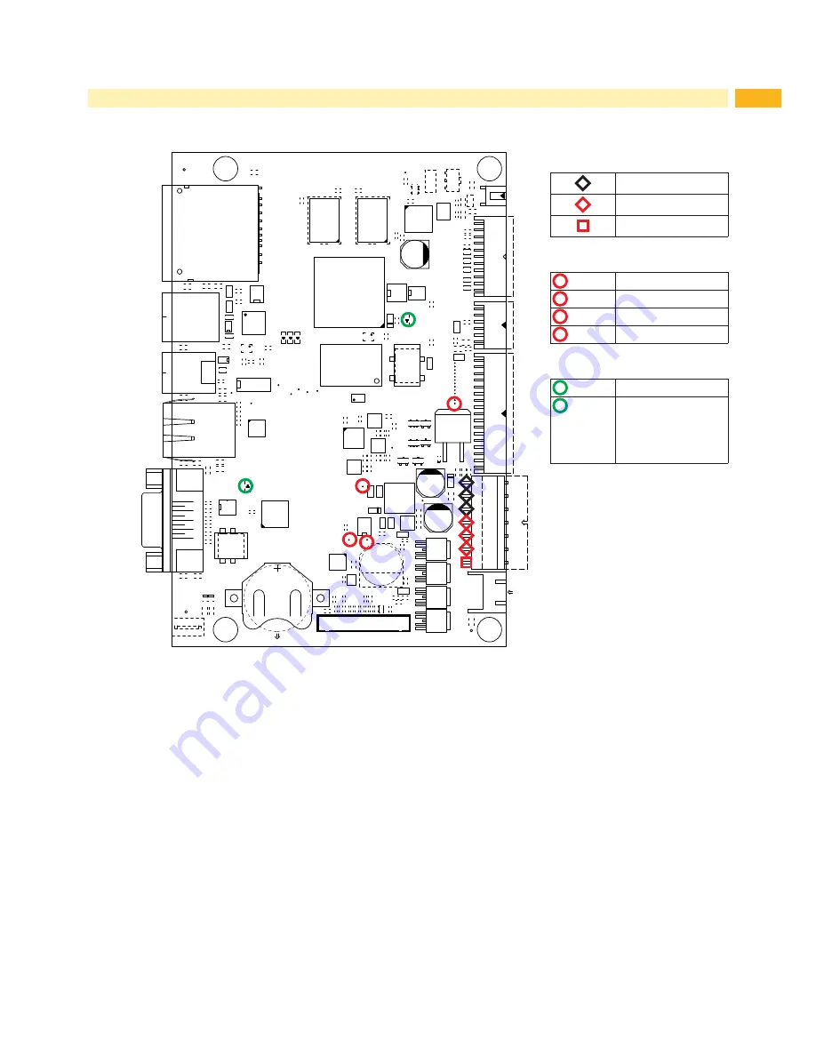
Layout Diagram PCB CPU
1
L6
12
R
130
L57
C185
R
323
B6
22
C3
91
R37
P6
R
131
R33
R
159
2
R
304
V19
1
G
B
+
C1
3
K
R
61
R220
V1
1
G
X1
V
M
R
305
TOP21
N
R22
C14
R
268
L2
7
1
V1
R
64
L12
AC
C16
V
18
9
C205
C208
10
R
270
C
341
L
B3
A1
C73
C
255
20
C
211
4
R169
5
C192
C
256
L43
L15
C214
1
R70
1
15
C2
46
C193
+
C
215
V12
A
A
P9
N6
TOP25
C2
59
R96
C194
L
C216
E
C26
D
L21
K
TOP16
AA
C264
R
D4
C217
U1
V24
T
R97
V1
5
L60
C
272
L50
3
C
224
C
221
TOP7
R60
D
L70
L61
C262
13
C276
CO
N1
C
223
R170
P
K
1
23
R1
L62
R140
C
17
C279
C
201
8
L31
C289
R84
4
K
L63
C8
C280
U7
18
C202
CD
R107
R
126
C6
C
C1
0
3
1top
W
P
C
203
C232
1
R141
U8
C
K
TOP11
P
R89
H
R4
C1
1
B
uch
se
L29
TOP5
H
C
210
N
R72
AE
R68
R
65
T
C235
L83
R
237
W
R5
C
212
C
291
2
R
74
R4
2
R
73
L5
6
G
1
C242
C
292
1
R168
R122
TOP26
16
L13
C234
#FD2
Gn
25
C2
82
C324
R
99
F1
C240
11
TOP17
C2
86
L73
R213
21
P5
L3
V14
A
2
F
R
19
9
C243
C321
+
E
R119
R219
F
TOP1
U
L
L56
M
R
56
R120
D3
L64
R87
AB
C252
R
572
TOP20
C198
8
L53
C1
2
9
R88
R25
L10
K
R
573
C200
19
R
100
R
574
R48
4
L37
L24
R
101
B2
N5
D15
14
R
575
CO
N1
0
L38
TOP14
24
D2
P8
2
1
R47
1
R
137
TOP9
J
R
568
R116
D
TOP4
C153
C
R
27
U3
J
R
66
C
263
D13
Y
C342
C113
P
F2
K
R
571
C
15
4
R
R29
L48
R
69
TOP15
C
270
C
314
2
L2
C
348
C155
C
L18
C
265
12
C116
R102
N
R6
K
2
TOP23
C
15
6
22
C293
L71
L3
3
3
C1
48
C
260
R121
C266
C
15
2
7
C1
L51
C1
49
C
320
CO
N2
17
L93
P2
R142
C
16
1
R
132
L34
C9
L39
C
258
B
U2
2
C1
84
GN
D
R123
R
256
R
35
CO
N1
2
C
16
2
A
R59
B
N
R117
G
R215
1
R7
5
C
261
G
R125
L68
M
C2
C28
C163
AC
D14
R71
CO
N4
R
108
V
R136
C187
C3
07
R
166
1
L90
V13
V7
C
16
4
C5
5
R280
F
R77
C3
08
L25
R160
C
213
C
160
15
C
207
2
R253
V21
R
139
C4
2
C
204
1
R163
C169
L42
L80
TOP6
C
268
CO
N1
7
10
C15
R
209
R78
C271
3
L14
#FD3
C
170
N1
R
98
C196
20
1
P4
CO
N9
C
225
C209
C309
1
U4
R171
L66
H1
R
31
C
17
1
K
8
L1
C
313
25
R85
E
C310
T
R172
K
B5
C27
C
351
C
17
2
R150
L30
C
352
L
R2
C
325
C
220
C311
L59
R
227
V9
C
168
AA
C
112
7
R
58
R303
R3
C
302
C312
C
15
8
8
C
183
C175
R158
J
TOP19
C
199
C267
V10
18
C
304
K
C345
C
15
9
R254
L9
C180
C
17
6
L58
C
206
3
V
20
2
C322
C346
C
16
6
R255
E1
C181
C
17
7
13
C3
N4
C323
C347
C
16
7
23
V25
R
20
R245
P7
C182
C
17
8
R
23
B1
C285
14
H
R
76
C
C349
C1
14
TOP22
G2
R247
CO
N5
C
150
C
17
4
B
R
62
R
26
H
C4
W
N
L16
V2
C230
C237
C350
R4
1
P
L28
R566
V17
C
151
R
63
H7
B4
C283
C335
AD
C
231
C239
R567
B
C222
R
301
TOP13
11
D5
M
L89
R1
55
A2
H4
L17
TOP8
21
1
C
338
C2
75
L72
L40
C241
1
D1
6
R
298
C
186
C327
L74
C274
C339
L49
TOP3
16
C245
P1
TOP24
C278
H5
E
C
340
1
1bot
GN
D
1
L20
G6
C300
R
299
C2
88
C6
6
M
F
R
24
F
L
CO
N3
CO
N1
1
AB
C
303
H6
C7
7
C
343
U
R11
L69
L67
A
R
294
R
300
R55
C157
4
C
344
1
E
2
14
C301
TOP12
C
165
C290
L23
R
1
L36
24
R134
C
277
C
197
+
C
173
C296
L75
R
236
9
1
C295
R
109
R
36
C179
19
C297
P3
L87
L32
R
295
R4
4
N2
1
D
7
C
219
AE
D
R
L35
L84
J
R4
5
R
32
N3
J
C
287
#FD1
P
AD
TOP2
1
Y
R
34
C269
K
CO
N8
L26
C
299
3
C72
7
R
30
R151
H
R
569
R54
L4
V3
CON7
17
R21
1
T
Ye
TOP10
R111
R152
TOP18
2
R
570
L52
L85
CON1
3
Measuring points of CON9:
GND
+24V
+V
MOT
(+24V)
Measuring point on the PCB:
TOP2
+24V
TOP3
+5V
TOP25
+24V TPH
TOP26
+V
MOT
(+24V)
LED on the PCB:
H1
+3,3V
H7
LED FPGA
on during start
procedure
blinking after the start
procedure
Fig. 15
Layout Diagram PCB CPU