Document type:
Title:
Revision date:
Revision:
User's Manual (MUT)
Mod. V1724 8 Channel 14bit - 100MS/s Digitizer
06/11/2007
7
NPO:
Filename:
Number of pages:
Page:
00103/05:V1724x.MUTx/07 V1724_REV7.DOC
63
17
3.2. Clock
Distribution
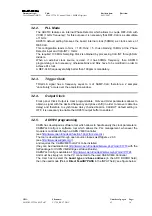
Fig. 3.3: Clock distribution diagram
The module clock distribution takes place on two domains: OSC-CLK and REF-CLK; the
former is a fixed 50MHz clock provided by an on board oscillator, the latter provides the
ADC sampling clock.
OSC-CLK handles both VME and Local Bus (communication between motherboard and
mezzanine boards; see red traces in the figure above).
REF-CLK handles ADC sampling, trigger logic, acquisition logic (samples storage into
RAM, buffer freezing on trigger) through a clock chain. Such domain can use either an
external (via front panel signal) or an internal (via local oscillator) source (selection is
performed via dip switch SW1, see § 2.6); in the latter case OSC-CLK and REF-CLK will
be synchronous (the operation mode remains the same anyway).
REF-CLK is processed by AD9510 device, which delivers 6 clock out signals; 4 signals
are sent to ADCs, one to the trigger logic and one to drive CLK-OUT output (refer to
AD9510 data sheet for more details:
http://www.analog.com/UploadedFiles/Data_Sheets/AD9510.pdf
); two operating modes
are foreseen:
Direct Drive Mode
and
PLL Mode
3.2.1. Direct
Drive
Mode
The aim of this mode is to drive externally the ADCs' Sampling Clock; generally this is
necessary when the required sampling frequency is not a VCXO frequency submultiple.
The only requirement over the SAMP-CLK is to remain within the ADCs' range.


