Document type:
Title:
Revision date:
Revision:
User's Manual (MUT)
Mod. V1724 8 Channel 14bit - 100MS/s Digitizer
06/11/2007
7
NPO:
Filename:
Number of pages:
Page:
00103/05:V1724x.MUTx/07 V1724_REV7.DOC
63
36
3.8.
Test pattern generator
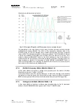
The FPGA AMC can emulate the ADC and write into memory a ramp (0, 1, 2, 3,…3FFF,
3FFF, 3FFE.., 0) for test purposes. It can be enabled via Channel Configuration register,
see § 4.12.
3.9.
Reset, Clear and Default Configuration
3.9.1. Global
Reset
Global Reset is performed at Power ON of the module or via a VME RESET (SYS_RES),
see § 4.44. It allows to clear the data off the Output Buffer, the event counter and
performs a FPGAs global reset, which restores the FPGAs to the default configuration. It
initialises all counters to their initial state and clears all detected error conditions.
3.9.2. Memory
Reset
The Memory Reset clears the data off the Output Buffer.
The Memory Reset can be forwarded via either a write access to Software Clear Register
(see § 4.45) or with a pulse sent to the front panel Memory Clear input (see § 3.6).
3.9.3. Timer
Reset
The Timer Reset allows to initialize the timer which allows to tag an event. The Timer
Reset can be forwarded with a pulse sent to Trigger Time Tag Reset input (see § 3.6).
3.10. VMEBus
interface
The module is provided with a fully compliant VME64/VME64X interface (see § 1.1),
whose main features are:
−
EUROCARD
9U
Format
−
J1/P1 and J2/P2 with either 160 pins (5 rows) or 96 (3 rows) connectors
−
A24, A32 and CR-CSR address modes
−
D32, BLT/MBLT, 2eVME, 2eSST data modes
−
MCST write capability
−
CBLT data transfers
−
RORA
interrupter
−
Configuration
ROM
3.10.1. Addressing
capabilities
3.10.1.1. Base
address
The module works in A24/A32 mode. The Base Address of the module can be fixed
through four rotary switches (see § 2.6) and is written into a word of 24 or 32 bit.
The Base Address can be selected in the range:
0x000000
ÅÆ
0xFF0000 A24
mode


