Snowball board System
Architecture and Design
46
8.7. PoP Memory Device
The A9500 Nova processor uses what is called PoP (Package-on-Package) memory. The memory
mounted on top of the Nova A9500 processor is a Low Power DDR2-SDRAM. Figure 8.13 shows
the PoP Memory concept.
Figure 8.13. PoP Memory
8.8. System Clocks
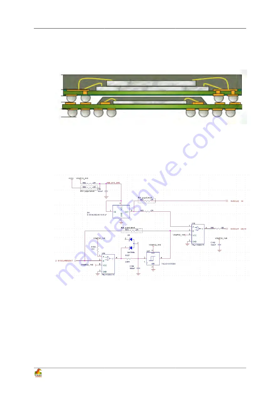
There are two clocks needed for operation of the Snowball board, 32kHz, 38.4MHz.
Figure 8.14 is a functional block diagram.
Figure 8.14. System clocks
8.8.1. 32Khz Clock
The AB8500 32Khz oscillator is used for the RTC, ADC of the coulomb counter and the internal PLL
(ULP) embedded into the AB8500. The AB8500 provides two 32Khz clock outputs: one dedicated
for the A9500 Nova processor and one used by the azurewave AW-NH580 combo module.
8.8.2. 38.4Mhz Clock
The 38.4Mhz oscillator is driven by the SYSCLKREQOUT output of the AB8500. At the end of the
power-up sequence the SYSCLKREQOUT output goes high and enables the 38.4MHz oscillator. This
oscillator provides a 38.4Mhz clock to the SYSCLK input of the AB8500 and the SYSCLK input of
Summary of Contents for SKY-S9500-ULP-CXX
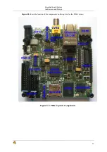
Page 1: ...SKY S9500 ULP CXX aka Snowball PDK SDK Hardware Reference Manual Revision 1 0 July 1 2011...
Page 3: ...SKY S9500 ULP CXX aka Snowball PDK SDK 3...
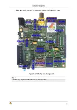
Page 17: ...Snowball board Overview 8 Figure 4 2 Snowball board Usage Scenarios...
Page 89: ...Connnector Pinouts and Cables 80 Figure 9 17 Location of R77...
Page 92: ...Mechanical Information 83 Figure 11 2 Board Mechanical drawing...
Page 93: ...Troubleshooting 84 Chapter 12 Troubleshooting 12 1 TBD TBD...
Page 94: ...Known Issues 85 Chapter 13 Known Issues TBD...
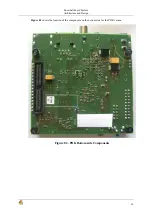
Page 96: ...PCB Component Locations 87 Figure 14 2 Snowball board Bottom Side Components...
Page 97: ...Schematics 88 Chapter 15 Schematics Figure 15 1 AB8500 1 2...
Page 98: ...Schematics 89 Figure 15 2 AB8500 2 2...
Page 99: ...Schematics 90 Figure 15 3 Power circuitry and serial port...
Page 100: ...Schematics 91 Figure 15 4 AP9500 1 4...
Page 101: ...Schematics 92 Figure 15 5 AP9500 2 4...
Page 102: ...Schematics 93 Figure 15 6 AP9500 3 4...
Page 103: ...Schematics 94 Figure 15 7 AP9500 4 4...
Page 104: ...Schematics 95 Figure 15 8 Reset circuitry and Audio in out...
Page 105: ...Schematics 96 Figure 15 9 HMDI circuitry...
Page 106: ...Schematics 97 Figure 15 10 Sensors...
Page 107: ...Schematics 98 Figure 15 11 WLAN Bluetooth GPS...
Page 108: ...Schematics 99 Figure 15 12 eMMC and microSD...
Page 109: ...Schematics 100 Figure 15 13 Expansion connector...
Page 110: ...Schematics 101 Figure 15 14 Ethernet 10 100M...


