background image

Snowball board System

Architecture and Design

55

8.15. HDMI Interface

The video output of the Snowball board is available on the HDMI connector. The HDMI output is
provided by the AV8100 which is a low power combo video HDMI and CVBS transmitter. The DSI
digital input interface of the AV8100 is interfaced on one of three MIPI DSI (MIPI-DSI2) offered by
the A9500 processor.

Figure 8.19 illustrates the HDMI interface design

Figure 8.19. HDMI interface design

8.15.1. Processor MIPI-DSI Interface

The  main  driver  for  the  HDMI  interface  originates  at  the  processor  via  the  DSI2  bus.  The  A9500
provides  the  signals  (1  clock  lane  and  2  data  lanes)  on  the  DSI2  bus  used  by  the  AV8100HDMI
transmitter  chip.  There  are  four  signals  used  to  control  the  HDMI  transmitter  that  originate  at
the  processor.  These  are  I2C0_SDA,  I2C0_SCL,  GPIO_192  (HDTV_INTn  signal)  and  GPIO_196
(HDTV_RST signal).

Summary of Contents for SKY-S9500-ULP-CXX

Page 1: ...SKY S9500 ULP CXX aka Snowball PDK SDK Hardware Reference Manual Revision 1 0 July 1 2011...

Page 2: ...e returned within 30 days from the date of delivery for a full refund THE FOREGOING WARRANTY IS THE EXCLUSIVE WARRANTY MADE BY SELLER TO BUYER AND IS IN LIEU OF ALL OTHER WARRANTIES EXPRESSED IMPLIED...

Page 3: ...SKY S9500 ULP CXX aka Snowball PDK SDK 3...

Page 4: ...TAG Connector 13 5 20 MIPI Debug Connector 13 5 21 RS232 13 5 22 Expansion connector 13 5 23 Electrical Specifications 14 6 Product Contents 15 6 1 Snowball board In The Box 15 6 2 Software On the Sno...

Page 5: ...32Khz Clock 46 8 8 2 38 4Mhz Clock 46 8 9 USB OTG Port 47 8 9 1 USB OTG Overview 47 8 9 2 USB OTG Design 47 8 9 3 OTG ULPI Interface 47 8 9 3 1 A9500 Interface 48 8 9 3 2 AB8500 Interface 49 8 9 4 OT...

Page 6: ...n Connector 64 9 Connnector Pinouts and Cables 68 9 1 Power Connector 68 9 2 USB OTG 68 9 3 CVBS Video 69 9 4 HDMI 69 9 5 Audio Connections 70 9 6 Audio Out 71 9 7 JTAG 72 9 8 MIPI Debug Connector 73...

Page 7: ...e Components 33 8 3 PDK Bottom side Components 34 8 4 SDK Top side Components 35 8 5 Input Power Section 36 8 6 VBAT Power Conditioning 38 8 7 VBAT Power Conditioning 39 8 8 Peripheral Voltages 40 8 9...

Page 8: ...al drawing 83 14 1 Snowball board Top Side Components 86 14 2 Snowball board Bottom Side Components 87 15 1 AB8500 1 2 88 15 2 AB8500 2 2 89 15 3 Power circuitry and serial port 90 15 4 AP9500 1 4 91...

Page 9: ...nsors 52 8 4 microSD A9500 Signals 53 8 5 A9500 Audio Signals 54 8 6 AB8500 Audio Signals 54 8 7 Processor MIPI DSI Interface 56 8 8 AV8100 Interface Signals 57 8 9 JTAG Signals 61 8 10 60 pin Expansi...

Page 10: ...box Hookup Describes how to connect the various cables to the Snowball board System Architecture and Design Provides information on the overall architecture and design of the Snowball board This is a...

Page 11: ...Introduction 2 Snowball board Schematics Describes the schematics of the Snowball board Snowball board PCB Information Describes the main features of the Snowball board PCB...

Page 12: ...ange History 3 Chapter 2 Change History Table 2 1 tracks the changes made for each revision of this document Table 2 1 Change History Rev Changes Date By 1 0 Initial release of the manual 07 01 2011 G...

Page 13: ...and Sync DA Digital to Analog DC Direct Current DDR Double Data Rate DDRSDRAM Double Data Rate Synchronous Dual Access Memory DENC Digital ENCoder DSI Display Serial Interface eMMC Embedded Multimedi...

Page 14: ...ea Network LCD Liquid Crystal Display LDO Low Drop out regulator LED Light emitting Diode LP Low pass MiPi Mobile Industry Processor Interface MP3 MPEG 1 Audio Layer 3 MPEG Moving Picture Experts Grou...

Page 15: ...pment Kit SOC System on a Chip SRAM Static RAM SWTX Switched TX An operation mode in the ITP software TMDS Transition Minimized Differential Signaling TX Transmitter UART Universal Asynchronous Receiv...

Page 16: ...0 dual core ARM registered trademark of ARM Limited application processor Dual Cortex A9 Mali 400 GPU Snowball board targets hobbyists and professional developers wanting to prototype new embedded des...

Page 17: ...Snowball board Overview 8 Figure 4 2 Snowball board Usage Scenarios...

Page 18: ...21 XOR HE10 2X5 Header HS USB OTG Mini AB USB connector Mini AB USB connector Audio Audio out in on 3 5mm jack connector Audio out in on 3 5mm jack connector Memory card microSD socket microSD socket...

Page 19: ...ed on the Snowball board and is mounted on top of the processor as previously indicated The key function of the PoP memory is to provide 8Gbits Mobile LPDDR2 SDRAM x32 for the SDK version 8Gbits Mobil...

Page 20: ...ereo output audio jack is provided to access the stereo output of the onboard audio CODEC The audio CODEC is embedded in the AB8500 The audio output available on this jack connector is the headset out...

Page 21: ...and 3D Magnetometer LSM303DLHC 3D Gyrometer L3G4200D Pressure sensor LPS001WP 5 14 microSD Card Connector A single microSD connector is provided as a means for the main non volatile memory storage on...

Page 22: ...f the board by using various JTAG emulators The interface is at 1 8V on all signals Only 1 8V levels are supported Warning DO NOT expose the JTAG header to 3 3V 5 20 MIPI Debug Connector A 34 pin conn...

Page 23: ...age USB 5 V Current DC Input Voltage DC 5 V Current DC TBD mA Expansion voltage 4 8 V USB OTG High Speed Mode 480 MBits s Full Speed Mode 12 MBits s Low Speed Mode 1 5 MBits s RS232 Transmit RS232 Hig...

Page 24: ...tion describes what comes in the box when a Snowball board is purchased 6 1 Snowball board In The Box The packaged product contains the following 1x Box 1x Snowball board in an ESD Bag Note No cables...

Page 25: ...Product Contents 16 Figure 6 2 Box Contents 6 2 Software On the Snowball board Snowball board comes with pre installed U Boot and linux kernel For software see Igloocommunity org...

Page 26: ...cable is connected to the Snowball board Figure 7 1 USB OTG Connection If the OTG Port is to be used as a Host the ID pin must be grounded This means that you must have a 5 pin cable connected to the...

Page 27: ...ained from a hardware supplier You need to make sure the supply is a regulated 5V supply Figure 7 2 shows where to insert the power supply into the power jack Figure 7 2 DC Power Connection The power...

Page 28: ...Snowball board but can be obtained from a hardware supplier Warning When the Snowball board is supplied from a Li ion battery remove the jumper on J25 Header Figure 7 3 shows where to insert a li ion...

Page 29: ...TAG emulator can be used for advanced debugging by connecting it to the JTAG header on the Snowball board Only the 20 pin version of the JTAG is supported Figure 7 4 shows the connection of the JTAG c...

Page 30: ...to connect a debug and trace data acquisition system that supports Mobile Industry Processor Interface System Trace Protocol This connector is only mounted on the SDK version Figure 7 5 shows the conn...

Page 31: ...le The configuration is different between the two available versions of the Snowball board The SDK comes only with a mini b USB connector dedicated to the serial port Figure 7 6 shows where the usb ca...

Page 32: ...quired to connect to a PC The adapter will not plug directly into the PC and will require an external Female to Female twisted cable Null Modem in order to connect it to the PC The ribbon cable is not...

Page 33: ...A cable can be connected to the Snowball board and from there it can be connected to a TV or monitor that supports a CVBS input This cable is not supplied with the Snowball board Figure 7 8 shows the...

Page 34: ...order to connect the HDMI output to a TV or monitor an HDMI cable is required This cable is not supplied with the Snowball board but can be obtained from a hardware supplier Figure 7 9 shows the prope...

Page 35: ...h as external stereo powered speakers can be connected to the Snowball board via a 3 5mm jack The audio cables are not provided with Snowball board but can be obtained from a hardware supplier Figure...

Page 36: ...red microphone or the audio output of a PC or MP3 player can be connected to the via a 3 5mm jack The audio cables are not provided with Snowball board but can be obtained from a hardware supplier Fig...

Page 37: ...that the Snowball board is supplied either from the DC Input or from the USB OTG One of them User LED can be controlled by the software The charger LED indicates the status of the charger The Blue LE...

Page 38: ...e are three buttons on the Snowball board the RESET button forces a full board reset and the USER button is used by the SW for user interaction The third button is the ON OFF button Figure 7 13 shows...

Page 39: ...Connection The microSD uses a push push connector for the insertion and removal of the microSD card The connector is mounted on the top side of the board Figure 7 14 shows the location of the microSD...

Page 40: ...n order to use the functionalities of the Azurewave AW NH580 combo module the user has to connect antennas on the two micro Coaxial Receptacles One for the Wifi BT and the other for the GPS Figure 7 1...

Page 41: ...nowball board System Architecture and Design This section provides a high level description of the design of the Snowball board and its overall architecture 8 1 System Block Diagram Figure 8 1 is the...

Page 42: ...Snowball board System Architecture and Design 33 Figure 8 2 shows the location of the components on the top side for the PDK version Figure 8 2 PDK Top side Components...

Page 43: ...Snowball board System Architecture and Design 34 Figure 8 3 shows the location of the components on the bottom side for the PDK version Figure 8 3 PDK Bottom side Components...

Page 44: ...em Architecture and Design 35 Figure 8 4 shows the location of the components on the top side for the SDK version Figure 8 4 SDK Top side Components Note There is no key components on the solder side...

Page 45: ...lustrates the design of the main power input section Figure 8 5 Input Power Section 8 2 1 USB DC Source The USB specification requires that the current consumed prior to enumeration be limited to 100m...

Page 46: ...lug with a center hot configuration If you are using the USB HUB or Ethernet interface additional current is required In the event that a higher DC load is required due to the addition of a daughterbo...

Page 47: ...et and Power Management The AB8500 supplies several key functions on the Snowball board This section covers a portion of those functions centered on the power and reset functions Included in this sect...

Page 48: ...ssor via the I2C interface I2C_APE_SDA SCL is used to control the AB8500 device 8 4 3 VARM The Varm DC DC converter supplies the ARM processor This DC DC converter supports voltage scaling feature and...

Page 49: ...DC converter supplies the A9500 internal logic 8 4 8 VBBN VBBP VBBN LDO and VBBP LDO provide the CPU biasing voltage to optimize the A9500 power consumption 8 5 Peripheral Voltages There are five add...

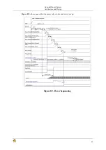
Page 50: ...ke sure that prior to installing the battery that R77 is removed 8 5 7 Power sequencing The AB8500 power supplies start up sequence is configurable through OTP The followings are the supplies and sign...

Page 51: ...Snowball board System Architecture and Design 42 Figure 8 9 is the sequence that the power rails clocks and reset come up Figure 8 9 Power Sequencing...

Page 52: ...es the PORDB8500n reset signal to the A9500 APE The A9500 resets the AB8500 through the ResetAB8500n reset signal On the other hand the Snowball board can be reset either from the reset push button or...

Page 53: ...ectivity is limited to the PoP memory access on the top of the processor and therefore is only accessible by the LP DDR2 SDRAM memory Two LP DDR2 SDRAM banks 0 and 1 are mapped into two consecutive 51...

Page 54: ...f LCDs The logic levels of the LCD signals are 1 8V so it will require buffering of the signals to drive most of the LCD diplay The LCD bus on the Snowball board is available on the 120 pin expansions...

Page 55: ...ck diagram Figure 8 14 System clocks 8 8 1 32Khz Clock The AB8500 32Khz oscillator is used for the RTC ADC of the coulomb counter and the internal PLL ULP embedded into the AB8500 The AB8500 provides...

Page 56: ...s hosts An example might be connecting a USB keyboard or printer to a Snowball board or a USB printer that knows how to grab documents from certain peripherals and print them The USB OTG compatible de...

Page 57: ...ster data in the ULPI PHY 8 9 3 1 A9500 Interface The controller for the ULPI interface is the Processor It provides all of the required signals to drive the interface Table 8 1 describes the signals...

Page 58: ...USB Data bit 5 In Out C20 ULPIDATA6 HS USB Data bit 6 In Out C21 ULPIDATA7 HS USB Data bit 7 In Out B20 8 9 4 OTG Charge Pump When the AB8500 acts as an A device a DC DC step up converter is used to p...

Page 59: ...d applications where performance flexibility ease of integration and system cost control are required The LAN9221 LAN9221i has been specifically designed to provide high performance and throughput for...

Page 60: ...oth GPS combo Module It supports standard interface SDIO v1 10 4 bit and 1 bit for WLAN High speed UART interface for BT FM GPS host controller interface and PCM I2S for BT FM audio data Warning In th...

Page 61: ...e sensors located on the I2C2 bus Table 8 3 provides the I2C addresses of the different sensors available on the Snowball board Table 8 3 I2C Sensors Part number Type I2C address LSM303DLHC 3D Acceler...

Page 62: ...MC0_DAT31DIR SD MMC data1 data3 direction Out AB3 8 13 1 microSD Power The microSD connector is supplied power from the AB8500 using the VAUX3 rail The maximum current this rail can provide is 400mA...

Page 63: ...ata through the two digital interfaces at a fixed 48 kHz rate in different formats with up to 8 channels per interface AudioIF 0 can also operate in burst mode that means audio data are collected in b...

Page 64: ...DSI2 offered by the A9500 processor Figure 8 19 illustrates the HDMI interface design Figure 8 19 HDMI interface design 8 15 1 Processor MIPI DSI Interface The main driver for the HDMI interface orig...

Page 65: ...clock line used to communicate with the AV8100 Out C15 GPIO_192 Interrupt input In GPIO_196 AV8100 Power Down control Out 8 15 2 AV8100 Power The AV8100 is supplied from the Vbat rail and VSMPS2_1V8 r...

Page 66: ...15 4 2 INT The INT signal from the AV8100 is wired to the A9500 processor GPIO_192 pin 8 15 5 HDMI Connector The Snowball board is equiped with a standard HDMI receptacle connector The Cable is not su...

Page 67: ...otocol that provides high level control functions between all of the various audiovisual products in a users environment It has been specified to operate at low speeds with minimal processing and memo...

Page 68: ...he serial port is no longer available on most PCs the Snowball board is equiped with a FT232R which is a USB to serial UART converter Consequently the serial port dedicated to the console is accessibl...

Page 69: ...r to the Snowball board but only that it is active 8 18 2 User LED There is one user LED LD1 which can be driven directly from the GPIO_142 pin on the processor These can be used for any purpose by th...

Page 70: ...nced debugging on the Snowball board by using a JTAG based debugger Figure 8 23 shows the interconnection to the A9500 processor Figure 8 23 JTAG Interface 8 19 1 A9500 Interface The JTAG interface co...

Page 71: ...pin expansion header As the A9500 has a multiplexing feature multiple signals can be connected to certain pins to add additional options as it pertains to the signal available The different columns in...

Page 72: ...LCD_D21 SM_ADQ5 MC5_FBCLK 38 GPIO128 MC2_CLK SM_CKO 39 GPIO92 LCD_D22 SM_ADQ6 MC5_CLK 40 GPIO94 KP_07 SM_ADVn MC5_DAT5 41 GPIO93 LCD_D23 SM_ADQ7 MC5_DAT4 42 GPIO97 KP_I6 SM_WEn MC5_DAT7 43 GPIO138 MC...

Page 73: ...e 8 11 shows what other signals can be accessed by setting the mux control register in the A9500 Table 8 11 120 pin Expansion Connector Signals Pin MUX 1 MUX 2 MUX 3 MUX 4 1 VBAT 2 VBAT 3 HFLP 4 SYSCL...

Page 74: ...P_O8 48 GPIO136 MC2_DAT5 SM_ADQ13 49 GPIO149 IP_GPIO0 SM_CS1n SM_PS1n 50 GPIO135 MC2_DAT4 SM_ADQ12 51 GPIO95 KP_I7 SM_CS0n SM_PS0n 52 GPIO134 MC2_DAT3 SM_ADQ11 53 PM_GPIO40 54 GPIO133 MC2_DAT2 SM_ADQ1...

Page 75: ...1 GPIO84 LCD_D14 KP_I5 92 GPIO6 U1_CTSn I2C1_SCL IP_GPIO0 93 GPIO85 LCD_D15 KP_I4 94 GPIO7 U1_RTSn I2C1_SDA IP_GPIO1 95 GPIO153 KP_I7 LCD_D24 U2_RXD 96 GPIO162 97 GPIO154 KP_I6 LCD_D25 U2_TXD 98 NC 99...

Page 76: ...Snowball board System Architecture and Design 67 Pin MUX 1 MUX 2 MUX 3 MUX 4 117 GPIO67 LCDB_CLK KP_I0 IP_GPIO7 118 CSI0_D1P 119 GND 120 GND...

Page 77: ...with the Snowball board 9 1 Power Connector Figure 9 1 illustrates the Snowball board power connector with the pin identified The supply must have a 2 0mm center hot connector with a 5 5mm outsider di...

Page 78: ...es the HDMI connector of the Snowball board Figure 9 4 HDMI Connector Table 9 1 is the pinout of the HDMI connector of the Snowball board Table 9 1 HDMI Pinout Pin Signal Name 1 TMDS Data2 2 TMDS Data...

Page 79: ...L 16 DDC_SDA 17 DDC CEC GND 18 5V 19 HPD 9 5 Audio Connections Figure 9 5 is the audio input jack required to connnect to the Snowball board Figure 9 5 Audio in Plug Figure 9 6 is the actual connector...

Page 80: ...Cables 71 9 6 Audio Out Figure 9 7 is the audio output jack required to connnect to the Snowball board Figure 9 7 Audio Out Plug Figure 9 8 is the actual connector used on the Snowball board Figure 9...

Page 81: ...in Signal Name Description I O 1 VSMPS2_1V8 Level voltage reference PWR 2 NC 3 TRST_n Test Reset IN 4 GND Ground PWR 5 TDI Test data input IN 6 GND Ground PWR 7 TMS Test mode select IN 8 GND Ground PW...

Page 82: ...each of the signals on the JTAG Header Table 9 3 JTAG Signals Pin Signal Name Description I O 1 VDEBUG_1V8 JTAG Debug Interface Reference Voltage PWR 2 TMS Test mode select IN 3 GND Ground PWR 4 TCK T...

Page 83: ...und PWR 24 TRC_DATA0 25 GND Ground PWR 26 TRC_DATA1 27 GND Ground PWR 28 TRC_DATA2 29 GND Ground PWR 30 TRC_DATA3 31 GND Ground PWR 32 TRC_EXT 33 GND Ground PWR 34 VDEBUG_1V8 Trace Interface Reference...

Page 84: ...Table 9 4 RS232 Signals Pin Signal Name I O 1 NC 2 NC 3 DRXD IN 4 NC 5 DTXD OUT 6 NC 7 NC 8 NC 9 GND PWR 10 VBAT PWR Figure 9 12 is the cable that is required in order to access the RS232 Header This...

Page 85: ...ough the USB interface On the PDK version the user will have to choose the terminal connector for the console by putting a jumper on the J24 header See the Table 9 5 below Table 9 5 RS232 configuratio...

Page 86: ...ototyping Header Table 9 6 Prototyping Header Pin MUX 1 MUX 2 MUX 3 MUX 4 1 VBAT 2 GPIO16 MSP0_RFS I2C1_SCL SLIM0_DAT 3 GPIO17 MSP0_RCK I2C1_SDA SLIM0_CLK 4 GPIO3 U0_TXD IP_TCK 5 GPIO2 U0_RXD IP_TMS 6...

Page 87: ...Connnector Pinouts and Cables 78 9 12 Backup Battery Installation Figure 9 15 is a picture of the backup battery Figure 9 15 Optional Backup battery...

Page 88: ...gure 9 16 Optional Backup battery Location Below are the steps required to install the backup battery Remove all cables from the board Remove R77 from the board as shown on Figure 9 17 Using Figure 9...

Page 89: ...Connnector Pinouts and Cables 80 Figure 9 17 Location of R77...

Page 90: ...81 Chapter 10 Snowball board Accessories 10 1 DC Power Supply TBD 10 2 LI ION Battery TBD 10 3 Serial Ribbon Cable TBD 10 4 USB HUBS TBD 10 5 HDMI Cables TBD 10 6 WIFI BT Antenna TBD 10 7 GPS Antenna...

Page 91: ...Mechanical Information 82 Chapter 11 Mechanical Information 11 1 Snowball board Dimensions Figure 11 1 Board Mechanical drawing...

Page 92: ...Mechanical Information 83 Figure 11 2 Board Mechanical drawing...

Page 93: ...Troubleshooting 84 Chapter 12 Troubleshooting 12 1 TBD TBD...

Page 94: ...Known Issues 85 Chapter 13 Known Issues TBD...

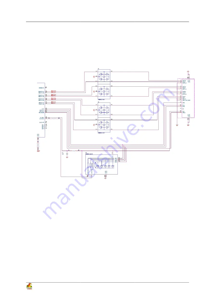
Page 95: ...ations 86 Chapter 14 PCB Component Locations Figure 14 1 and Figure 14 2 contain the top and bottom side components locations of the Snowball board on the Snowball board Figure 14 1 Snowball board Top...

Page 96: ...PCB Component Locations 87 Figure 14 2 Snowball board Bottom Side Components...

Page 97: ...Schematics 88 Chapter 15 Schematics Figure 15 1 AB8500 1 2...

Page 98: ...Schematics 89 Figure 15 2 AB8500 2 2...

Page 99: ...Schematics 90 Figure 15 3 Power circuitry and serial port...

Page 100: ...Schematics 91 Figure 15 4 AP9500 1 4...

Page 101: ...Schematics 92 Figure 15 5 AP9500 2 4...

Page 102: ...Schematics 93 Figure 15 6 AP9500 3 4...

Page 103: ...Schematics 94 Figure 15 7 AP9500 4 4...

Page 104: ...Schematics 95 Figure 15 8 Reset circuitry and Audio in out...

Page 105: ...Schematics 96 Figure 15 9 HMDI circuitry...

Page 106: ...Schematics 97 Figure 15 10 Sensors...

Page 107: ...Schematics 98 Figure 15 11 WLAN Bluetooth GPS...

Page 108: ...Schematics 99 Figure 15 12 eMMC and microSD...

Page 109: ...Schematics 100 Figure 15 13 Expansion connector...

Page 110: ...Schematics 101 Figure 15 14 Ethernet 10 100M...

Page 111: ...e 16 1 describes the main features of the PCB Table 16 1 PCB features Features Description Dimension 85mm X 85mm Material Panasonic R1566W R1551W FR4 150 TG Halogen Free Copper Finish Immersion Gold L...

Reviews: