background image

Summary of Contents for 142

Page 1: ...CalComp Model 140 Model 142 Floppy Disk Drives Technical Manual...
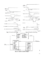
Page 2: ...MODEL 140 AND MODEL 142 FLOPPY DISK DRIVES TECHNICAL MANUAL April 1977 California Computer Products Inc 2411 W La Palma Anaheim CA 92801 Part No 10150 901 003 2...

Page 3: ...include the Model 142 and all versions of the Model 140 Incorporates the intent of Technical Bulletin D178 and Field Change Notice DFOOS Incorporates latest changes as per Small Disk Operations Copyri...

Page 4: ...d 3 2 Peak Shift Precompensation 3 3 Track Accessing 3 3 Read Data Timing 3 3 Write Data Timing 3 3 Power On to Data Transfer 3 6 Functional Areas 3 6 Control System 3 6 Positioning System 3 8 Read Wr...

Page 5: ...e 1 1 2 1 2 2 2 3 2 4 2 5 2 6 2 7 3 1 3 2 3 3 3 4 3 5 iv Group Assembly Parts List 5 1 Figure and Item Number 5 1 Part Number 5 1 Description 5 1 Quantity Per Assembly 5 1 Usage Code 5 1 Purchased Par...

Page 6: ...Logic Diagram 3 17 Stepper Motor Direction Sequencing 3 18 Decode and Current Drivers for 00 Code 3 18 Track 00 Detector Circuit 3 19 Write Channel Simplified Logic Diagram 3 20 Double Frequency Writ...

Page 7: ...ard Assembly VR56 5 17 Data and Control Board Assembly VR57 5 21 Data and Control Board Assembly VR58 5 25 Data and Control Board Assembly VR60 5 29 Data and Control Board Assembly VR82 5 33 Data and...

Page 8: ...ing the disk drives The information in this manual other than that contained in this section is divided into four basic sections Installation and Operation Uncrating Installation Operation Theory of O...

Page 9: ...5 00 inches add 3 inches for connector clearance 16 pounds 18 pounds shipping 100 to 240 vac 10 20 50 0 5 Hz or 60 0 5 Hz single phase 1 7 amperes maximum 60 Hz 1 7 amperes maximum 50 Hz 1 2 amperes m...

Page 10: ...equency frequency modulated FM 142 only Double frequency FM double density modified frequency modulation MFM FM 250 000 bits per second MFM 500 000 bits per second 2 microseconds 360 rpm 2 5 83 3 mill...

Page 11: ......

Page 12: ...d discard the fiberglass straps that secure the shipping container Note Do not lift the disk drive by the floppy disk loading handle as the handle can be damaged 2 Remove all parts from the shipping c...

Page 13: ...designed for ribbon cable which has press on connectors that plug into the interface connector board The part number for both the terminated and unterminated boards is 16292 001 however the terminated...

Page 14: ...ard see Figures 2 5 and 2 6 that provides line terminations for all inCOming signals to the disk drive The twisted pair connector board has feedthrough solder lands with two eyelets in each land Syste...

Page 15: ...Termination for Disk Drive Output Signals IUBOONCABLEINTERFAcE I 16292 001 VN45 Jl PI J I _ DISK DRIVE _ 1_ _ _ _ _ L ____ 1 T Jl PI 2200 Jl 5V _Af J 3300 LAST DISK DRIVE RIBBON CABLE INTERFACE J _ T...

Page 16: ...r board to verify proper pin assignments Refer to Table 2 2 6 Turn power off at the controller and connect the cables to the disk drives TABLE 2 2 TWISTED PAIR INTERFACE SIGNAL CABLE CONNECTIONS Signa...

Page 17: ...as a jumper between pins 4 and S Checkout The disk drive can be checked out operationally by running the disk drive either offline with the exerciser or online with the system 2 6 OPERATION Floppy dis...

Page 18: ...he location of the floppy disk opening for loading A FLOPPY DISK IN LOAD POSITION The procedure for loading unloading the floppy disk is as follows 1 2 3 4 5 Move the handle to the open position Inser...

Page 19: ......

Page 20: ...understood as a basis for more detailed study offunctional systems and circuits The following principles of operation provide this necessary background information The recording medium specified for...

Page 21: ...The tracks are numbered 00 thm 76 beginning with the track nearest the outer edge of the disk DATA NRZ MANCHESTER MFM DATA MFM FLUX REVERSALS o o D Data Recording Method Modified Frequency Modulation...

Page 22: ...nd T2 are both 310 nanoseconds low frequency or 232 nanoseconds medium frequency write pulse Bearly If nominal T1 and T2 are both 155 nanoseconds high frequency write pulse B on time Figure 3 3C defin...

Page 23: ...FECTS OF PEAK SHIFTING AND PRESTRESSING I Tl J I_ T2 I Tl T2 WRITE B EARLY J Tl I T2 I T1 T2 WRITE B LATE B EXAMPLES OF PRESTRESS DETER MINATION NOTE 0 MFM DATA MUST I I I I II II II I I II II II II I...

Page 24: ...e 3 4 Track Accessing Timing SELECT __________________________________ WRITE Jill ENABLE I RAW DATA Ie I II 1 II 1 I 300 NS I 4 2 US MAX tlOO NS I I I I I I 1 I I I I 1 4US I 2US I H 51 US 0 11 US 1 0...

Page 25: ...natory pur poses it is assumed that a cartridge is loaded and that the controller will wait for the READY interrupt before causing head stepping FUNCTIONAL AREAS The floppy disk drives contain three m...

Page 26: ...Ii II___t_l I I I J 250 US MIN I 30 MS MIN I I I I READ DATA t 1 1 11 l t LI Figure 3 10 Power On to Read Timing REAO WRITE SYSTEM FROM CONTROLLER SU BSYSTEMS FUNCTIONS WRITE DATA READ NJRITE LOGIC WR...

Page 27: ...k 3 8 An INDEX pulse occurs once per disk revolution TRACK 00 status is available for initializing the controller track address register This signal is developed form a photo transducer when the carri...

Page 28: ...induces a voltage across the coils of the electromagnet This voltage is amplified and conditioned to recover the recorded infor mation MECHANICAL SYSTEM The disk drive comprises the following mechani...

Page 29: ...sting to align the disk in the proper plane before it passes over the read write head 3 10 CENTERING CONE SPINDLE DRIVE _ J PULLEY A CENTERING CONE AND READ WRITE EAD UNLOADED CONE EXPANDER HEAD LOAD...

Page 30: ...between the major circuits are shown in Figure 3 17 Control Logic The control logic contained in the disk drives perform three functions Generates and detects index and sector pulses Monitors disk sp...

Page 31: ...me The output of the amplifier swings approxi mately 4 0 volts and is differentiated by C7 and R37 The negative transition triggers a 600 microsecond one shot The index transducer also detects sector...

Page 32: ...dex count pulses Both outputs are inhibited during power up time since the ramp period is greater than 198 milliseconds or 5 5 milliseconds see Figure 3 21 Disk Speed Monitor When power is applied to...

Page 33: ...POSITIONING CONTROL r ELECT RAWDATAl HD LOADED OUTPUT I RAW I I DATA I I I L ____ J I RAW TTL LEVELS I I READ CLOCK I I READ DATA I SEPARATED I L __ __________ D O U2 J WRITE ENABLED REAOJWRITE SELECT...

Page 34: ...LY 4 61T COUNTER SELECT A12 D _____ _ND_E_X l L J SELECT A12 4_________________________________ S EC T 0 R 1 Figure 3 18 Index Pulse Detection on Speed Monitor Simplified Logic Diagram 17V SV 5V R30 R...

Page 35: ...ead to a track in response to the controller issuing three signals Q6 RAMP SPEED SIGNAL 4 81T COUNTER C LINPUT 4 81T COUNTER CLKINPUT ONVERTED READY 1 ___11___ u 5V Figure 3 22 Head Load Relay Driver...

Page 36: ...rsed if the decoded sequence goes down from a count of 11 The two sequences are shown in Figure 3 26 Low order one shot A24 also provides the second step pulse that is required for 30 degree rotation...

Page 37: ...1 Out CCW 1 0 Out CCW 0 1 Out CCW 0 0 Out CCW When stepping is terminated the stepper motor is main tained in the last position by the binary decode holding a ground on one of the quadrature windings...

Page 38: ...Rl R2 R4 J7 R129 R7 R3 5V further step out positioning and simultaneously flags the controller by activating the TRACKOO status line The track 00 transducer circuit comprises a phototransistor a light...

Page 39: ...lied to the read side of the read write matrix to prevent any current flow through this channel Write Current Control When the write current control circuit is not in the write mode current flow is in...

Page 40: ...re 3 30 Double Frequency Write Control and Write Coils Current Flow o o o o o o 1 CP I L lE ____ fl ________ fl ________ fl ____ rl ________ fl ______ n ________ rl ________ n_______ WRITE FF Q ___ WR...

Page 41: ...current source and is directly controlled by WRITE ENABLE When enabled by the low level output of inverter AI3 through driver A3 erase current is turned on at the same time that WRITE ENABLE is activ...

Page 42: ...se pattern now exhibits a transition between 0 volt and 5 volts for every flux change recorded on the disk track Raw Data Output Gating The raw data output gating network Figure 3 34 consists of two d...

Page 43: ...n a data pulse is detected between clocks refer to Figure 3 37 G Flip flop A22 is set by the leading edge of a data pulse and is reset by the leading edge of the next clock in the raw data serial bit...

Page 44: ...on the power transistor thereby increasing or reducing load current READ DECODER WITH PLO ASSEMBLY The Read Decoder with PLO Assembly read decoder assembly contains the circuitry necessary to track an...

Page 45: ...GT goes high gate B is inhibited and gate C is enabled to pass DATA IN through to gate D see Figure 3 40 The leading edge of a DATA IN pulse will generate the same pulse from one shot E as did the WRT...

Page 46: ...percent to 93 percent and 7 percent respectively Since the outputs are effectively added this causes no change on pin 1 of operational amplifier Land consequently no change in the yeo Sync Up PLO Oper...

Page 47: ...n n GQ H LJ U LJ U U U U KQ U U U U 4F Ql Q2 LCPIN 1 Figure 3 41 PLO Sync Up o o 1 o 1 1 o o o WRITE DATA MFM WRITE TRANSITIONS L WRITE CLOCK READ TRANSITIONS READ DATA MFM DATA NRZ CLOCK Figure 3 42...

Page 48: ...the MFM recording scheme the clock bit occurs during the first half of the bit cell and a data bit occurs during the last half of the bit cell see Figure 3 46 By convention the incoming data are zero...

Page 49: ...1 I 0 I L 1 b C b K Figure 3 44 Data Decoder Waveforms 2F 3 30 READ SYNC FROM CONTROLLER E sHOT l I I I I 2F L _____ J 2F t READ DATA FROM DATA RECODER LOGIC CLOCK 2F Figure 3 45 Read Data Decoder Sy...

Page 50: ...rAfiJusr1 J 49 IF WINDOW o IF c A2 4 S AS ll AIO 9 BQ J 4S OQ TRIG BY POS TRANS J S AS 7 0 All 9 CQ 0 AIO 9 C A2 4 L tJ 0 0 CLOCK 5 u A7 6 A2 4l All 9l L tJ 0 AIO 5 FQ JLJL Jl n n IL11 D AIO 9 C AS 7...

Page 51: ...J u L J flLJrl_____O ____ O ___PL Jn _O____ O ____ O ___ TRANSITIONS END OF BIT CELL ONE S MIDDLE BIT CELL FROM CROSSOVER DETECTOR DATA AFTER ONE SHOT VCO 2 0 S MHz O S MHz AFTER ONE SHOT 60 7 SEC REA...

Page 52: ...per operation of each disk drive DISK DRIVE EXERCISER Maintenance checks and adjustment procedures can be performed online by using the controller or offline by using the Model 2140 Disk Drive Exercis...

Page 53: ...wo Position Switch In ENABLE position selects disk drive enabling I O gates In DISABLE position deselects disk drive Two Position Switch In LOAD position causes disk to contact head In UNLOAD position...

Page 54: ...the disk drive if required MAINTENANCE PROCEDURES The maintenance procedures are divided as follows Check Adjustment Replacement Note The cognizant maintenance personnel should read the entire check a...

Page 55: ...4v and one ac drive voltage are applied to the disk drive from the controller An internal shunt regulator develops a third dc level 17 volts 4 4 Voltage Checks WARNING Exercise extreme care when the c...

Page 56: ...Drive Belt Tension Adjustment To adjust drive belt tension proceed as follows 1 2 3 4 Turn ac power off Loosen the four drive motor mounting nuts see Figure 4 5 MOUNTING NUTS Figure 4 5 Drive Belt Che...

Page 57: ...exerciser to the disk drive and apply power Set the following switches on the exerciser to the positions indicated STEP COUNT All switches down HEAD LOAD to UNLOAD SELECT to DISABLE TRACK 43 to BELOW...

Page 58: ...ducer proceed as follows 1 Connect channel 1 of the oscilloscope to J6 4 2 3 Adjust the index LED located in the cone lift cover for maximum pulse amplitude Turn power off 4 Note The fo lowing step is...

Page 59: ...ectrical connections and ensuring that no short ing will occur 5 Connect the exerciser to the disk drive and apply power 6 7 4 8 Insert the hard sector alignment diskette and close the handle Set the...

Page 60: ...e upper and lower bearings by using hand pressure Remove the inner and outer bearing spacer and spring washer READJWRITE HEAD 6 7 8 Inspect all parts for wear and replace any defective part Clean the...

Page 61: ...is connected to the disk drive by a shoulder screw on either side that is inserted through coil springs When the shoulder screws are released the coil springs will fly out unless the cover is held in...

Page 62: ...ARM Figure 4 12 Head Load Check and Adjustment 4 Verify that the tang of the head load solenoid just contacts the load arm S If it is adjusted incorrectly set the Head Load Adjust screw Figure 4 12 f...

Page 63: ...ons indicated below HEAD LOAD to UNLOAD SELECT to ENABLE FUNCTION SELECT to ALT STEP STEP COUNT to 1 switch 1 up all others down CONTINUOUS SINGLE right side to CONTINUOUS Verify visually that the TRA...

Page 64: ......

Page 65: ...with the Model 140 is 15967 001 part number 17032 001 is used with the Model 142 The Data Decoder with PLO Board is normally installed in the controller To adjust the Data Decoder with PLO Board proce...

Page 66: ...parts used in the disk drives may be obtained directly from a vendor Purchased parts will also be supplied by CalComp on receipt of an order specifying the part number as shown in this section The in...

Page 67: ...e Code FIGURE AND ITEM NUMBER The figure number relates the parts list to its associated illustration The item number assigned to each part is shown on the illustration to show physical location PART...

Page 68: ...0 004 Disk Drive Unit Model 140C 240 vac 50 Hz REF K 14700 005 Disk Drive Unit Model 140C 100 vac 60 Hz REF L 14700 006 Disk Drive Unit Model 140C 208 vac 50 Hz REF M 14700 007 Disk Drive Unit Model 1...

Page 69: ...07 100 vac 50 Hz 008 208 vac SO Hz OXl 115 vac 60 Hz OX2 230 vac 60 Hz OX3 220 vae 50 Hz 18411 0XX 142 OX4 240 vac 50 Hz Model 142 r r r OX5 100 vae 60 Hz I OX6 208 vac 60 Hz Middle digit Last digit O...

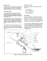
Page 70: ...16 20 21 32 F JgUIe 5 1 Model 140 and 142 DISk Drive Unit Sheet 2 of 2 Ii 29...

Page 71: ...rive Attaching Parts 5 16922 307 Screw Pan Hd 6 32 x 7 16 Lg 2 99357 004 Pin Dowel Nil NFS 2 91446 019 Spring Compression Nil NFS 11706 001 Button Handle Nil NFS 11703 001 Handle Molded Nil NFS 6 1358...

Page 72: ...mponents 17287 001 Board Assy Data Control VR83 U W Model 142 Options X AE OOX 02X 04X 05X refer to Figure 5 4F for components Attaching Parts 40 16922 307 Screw Pan Hd 6 32 x 7 16 Lg 7 ___ IIe ___ 41...

Page 73: ...C Drive 115v 60 Hz refer to Figure 5 3 A G P X for components 11694 002 Motor Assy AC Drive 230v 60 Hz refer to Figure 5 3 B H Q Y for components 11694 003 Motor Assy AC Drive 220v 50 Hz refer to Figu...

Page 74: ...01 Clip Cable 4 9 11714 001 Transducer Optical Emitter 1 Attaching Parts 10 90448 020 Screw Machine Pan Hd 6 32 x 3 8 Lg 2 11 90489 003 Lockwasher Split No 6 2 12 90488 004 Washer Flat 2 13 93719 003...

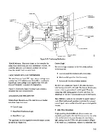
Page 75: ...17 5 23 Figure 5 2 Cone Lift Cover Assembly 5 9...

Page 76: ...Parts 4 90487 OO6 Nut Hexagon 4 5 90489 OO5 Lockwasher Split 4 6 90488 006 Washer Flat 4 7 90603 003 Terminal Ring Torque 8 90605 003 Connector Molex 3 Pin JOI 1 9 90440 002 Pin Connector 3 10 11648...

Page 77: ...see Figure 5 1 for REF K S AA NHA 11694 005 Motor Assy Ac Drive 10Ov 60 Hz see Figure 5 1 for REF C L T AB NHA 11694 006 Motor Assy Ac Drive 208v 60 Hz see Figure 5 1 for REF M U AC NHA 11694 007 Moto...

Page 78: ...Gate Non Invert Hex I Input TTL A3 All 2 22 10207 001 Amplifier Linear Diff Al 23 96758 001 Amplifier Linear Diff Comp A2 26 2 90355 332 CapaCitor 0033 uF 10 10Ov C7 1 18452 347 Capacitor Metal Poly...

Page 79: ...13 21 ____ 24 3 2 i Figure 5 4 Data and Control Board Assembly VR49 5 13...

Page 80: ...tor Molded 130 uH LA 90376 240 Inductor Molded 240 uH L3 1 90965 330 Inductor Molded 33 uH Ll 2 2 90343 001 Diode Low Capacitance CR4 14 17 19 21 15 90344 001 Diode Rectifier 1 Amp 50v CRI 1 90346 062...

Page 81: ...561 Resistor 560 ohm 5 1 4W RI7 20 78 5 90364 621 Resistor 620 ohm 5 1 4W R40 41 2 90364 682 Resistor 6 8K 5 1 4W R39 118 2 90364 751 Resistor 750 ohm 5 1 4W R8 26 34 3 90364 752 Resistor 7 5K 5 1 4W...

Page 82: ...e Non Invert Hex I Input TTL A3 All 2 22 10207 001 Amplifier Linear Diff Al 1 23 96758 001 Amplifier Linear Diff Comp A2 26 2 90355 332 Capacitor 0033 uF 10 100v C7 1 18452 347 Capacitor Metal Poly 04...

Page 83: ...21 i ro r 136 VR66 G J 3 2 1 Figure S 4A Data and Control Board Assembly VRS6 5 17...

Page 84: ...ctor Molded 130 uH 1A 90376 240 Inductor Molded 240 uH L3 1 90965 330 Inductor Molded 33 uH Ll 2 2 90343 001 Diode Low Capacitance CR4 14 17 19 21 15 90344 001 Diode Rectifier 1 Amp SOy CRI 1 90346 06...

Page 85: ...2 90364 561 Resistor 560 ohm 5 1 4W R17 20 78 5 90364 621 Resistor 620 ohm 5 1 4W R40 41 2 90364 682 Resistor 6 BK 5 1 4W R39 118 2 90364 751 Resistor 750 ohm 5 1 4W R8 26 34 3 90364 752 Resistor 7 5K...

Page 86: ...te Non Invert Hex I Input TTL A3 All 2 22 10207 001 Amplifier Linear Diff Al I 23 96758 001 Amplifier Linear DiffComp A2 26 2 90355 332 Capacitor 0033 uF 10 100v C7 1 18452 347 Capacitor Metal Poly 04...

Page 87: ...3 2 Figure 5 4B Data and Control Board Assembly VR57 5 21...

Page 88: ...ctor Molded 130 uH lA 90376 240 Inductor Molded 240 uH L3 1 90965 330 Inductor Molded 33 uH Ll 2 2 90343 001 Diode Low Capacitance CR4 14 17 19 21 15 90344 001 Diode Rectifier 1 Amp SOy CRI 1 90346 06...

Page 89: ...64 561 Resistor 560 ohm 5 1 4W R17 20 78 5 90364 621 Resistor 620 ohm 5 1 4W R40 41 2 90364 682 Resistor 6 8K 5 1 4W R39 118 2 90364 751 Resistor 750 ohm 5 I 4W R8 26 34 3 90364 752 Resistor 7 5K 5 1...

Page 90: ...Non Invert Hex I Input TTL A3 All 2 22 10207 001 Amplifier Linear Diff Al 1 23 96758 001 Amplifier Linear Diff Comp A2 26 2 90355 332 Capacitor 0033 uF 10 100v C7 1 18452 347 Capacitor Metal Poly 047...

Page 91: ...13 21 24 3 2 Figure S 4C Data and Control Board Assembly VRS8 5 25...

Page 92: ...tor Molded 130 uH IA 1 90376 240 Inductor Molded 240 uH L3 1 90965 330 Inductor Molded 33 uH Ll 2 2 90343 001 Diode Low Capacitance CR4 14 17 19 21 15 90344 001 Diode Rectifier 1 Amp SOy CRt 1 90346 0...

Page 93: ...364 561 Resistor 560 ohm 5 1 4W RI7 20 78 5 90364 621 Resistor 620 ohm 5 1 4W R40 41 2 90364 682 Resistor 6 SK 5 1 4W R39 liS 2 90364 751 Resistor 750 ohm 5 1 4W R8 26 34 3 90364 752 Resistor 7 5K 5 1...

Page 94: ...rt Hex I Input TTL A3 Al 1 2 22 10207 001 Amplifier Linear Diff A1 1 23 96758 001 Amplifier Linear Diff Comp A2 26 2 90355 332 Capacitor 0033 uF 10 100v C7 1 18452 347 Capacitor Metal Poly 047 uF 5 CI...

Page 95: ...3 2 1 Figure S 4D Data and Control Board Assembly VR60 5 29...

Page 96: ...ctor Molded 130 uH IA 90376 240 Inductor Molded 240 uH L3 1 90965 330 Inductor Molded 33 uH Ll 2 2 90343 001 Diode Low Capacitance CR4 14 17 19 21 15 90344 001 Diode Rectifier 1 Amp 50v CRI 1 90346 06...

Page 97: ...561 Resistor 560 ohm 5 1 4W R17 20 78 5 90 364 621 Resistor 620 ohm 5 1 4W R40 41 2 90364 682 Resistor 6 8K 5 1 4W R39 118 2 90364 751 Resistor 750 ohm 5 1 4W R8 26 34 3 90364 752 Resistor 7 5K 5 1 4...

Page 98: ...7 001 Gate Non Invert Hex I Input TTL A3 All 2 21 10207 001 Amplifier Linear Diff Al 1 22 96758 001 Amplifier Linear Diff Comp A2 26 2 90355 332 Capacitor 0033 uF 10 100y C7 1 18452 347 Capacitor Meta...

Page 99: ...11 IL L I 101 1q 01 1101 1101 18 cu I IOS to C10 1112 I S 1116 20 D R z 1 1 CI 02 23 Figure 5 4E Data and Control Board Assemblyt VR82 5 33...

Page 100: ...109 Resistor 105 ohm 1 1 8W R73 74 2 93952 026 Resistor 681 ohm 1 lW R75 80 2 17172 001 Diode Switching VHF UHF CR7 8 13 14 4 17102 062 Diode Zener 6 2v 400 mY CR20 1 90376 068 Inductor Molded 68 uH...

Page 101: ...126 2 90364 912 Resistor 9 1K 5 1 4W R37 1 90365 201 Resistor 200 ohm 5 lW R72 1 90365 680 Resistor 68 ohm 5 lW Rl 30 2 90365 821 Resistor 820 ohm 5 lW R91 1 90365 101 Resistor 100 ohm 5 lW Rl1 1 9036...

Page 102: ...001 Gate Non Invert Hex I Input TTL A3 All 2 21 10207 001 Amplifier Linear Diff Al 1 22 96758 001 Amplifier Linear Diff Comp A2 26 2 90355 332 Capacitor 0033 uF 10 100v C7 18452 347 Capacitor Metal P...

Page 103: ...11 c ell o 1 5 2 Figure S 4F Data and Control Board Assembly VR83 20 23 o o 5 37...

Page 104: ...90367 200 Resistor 196 ohm 1 1 8W R130 131 2 90367 228 Resistor 237 ohm 1 1 8W R86 90371 110 Resistor 100 ohm 5 5W R120 1 90376 068 Inductor Molded 68 uH Ll 2 3 4 4 90343 001 Diode Low Capacitance CR...

Page 105: ...90364 752 Resistor 7 5K 5 1 4W R29 90364 911 Resistor 910 ohm 5 1 4W R125 126 2 90364 912 Resistor 9 1K 5 1 4W R37 1 90365 201 Resistor 200 ohm 5 lW R72 1 90365 680 Resistor 68 ohm 5 1W Rl 30 2 90365...

Page 106: ...2 21 90354 101 Capacitor Mica 100 pF 5 500v Cll 14 2 22 90343 001 Diode Low Capacitance Switch CR5 7 3 23 90346 056 Diode Zener 5 6v VR5 24 90356 156 Capacitor Tantalum 68 uF 15v C12 25 90356 355 Capa...

Page 107: ...I I I 13 I Lii J R31 rm I o J I 12 R22 C36 VR4 I 11 Y J D VRe i4 A2 25 AI6 C26 R36 27 10 0 411 VR2 I 1 19 I r l AIU I R2I AI5 R20 li t 1 _ ___ 9 _ _ RI4 4 Q2 I I I I I I I 39 I 0 RI RI9 8 _ L 1 _ U I...

Page 108: ...1 90354 101 Capacitor Mica 100 pF 5 50Ov C11 14 2 22 90343 001 Diode Low Capacitance Switch CR5 7 3 23 90346 056 Diode Zener 5 6v VR5 24 90356 156 Capacitor Tantalum 68 uF 15v C12 25 90356 355 Capacit...

Page 109: ...California Computer Products Inc 2411 W La Palma Anaheim CA 92801...

Reviews:

Related manuals for 142