C. Data and ICB Interface Connectors
This appendix provides information that is helpful when interfacing to an MCA.
MCA Data Transfer
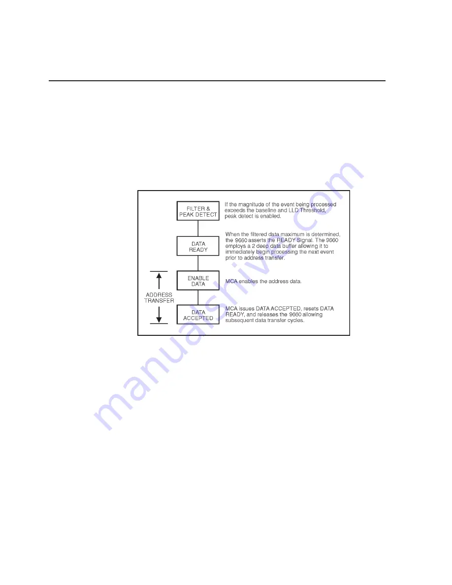
A typical conversion and data transfer sequence is illustrated below (Figure 37):
The result of the digitization and digital filtering is a 14-bit binary coded number or
address. At the conclusion of the conversion, the address data is transferred into a
holding register and the data transfer signal DATA READY is set true. The address
data is now valid and can be accessed and used by the MCA or CPU.
Due to a two-deep data buffer, the 9660 can begin processing the next event even
though data transfer to the memory unit is still in process.
The address lines are driven by tri-state drivers activated by ENABLE DATA, which
is initiated by the data memory device.
When transfer is complete, the memory device sets DATA ACCEPTED true, releasing
the 9660 to begin the next pending transfer sequence.
Appendix C - Data and ICB Interface Connectors
76
Model 9660-9660A ICB Digital Signal Processor
Figure 37 Typical Conversion and Transfer Sequence


