background image

Summary of Contents for A-200 series

Page 1: ... 230 V lViodeO SERVICE MANUAL Canon FEB 1985 SY8 0061 751 COPYRIGHT BY CANON INC CANON A 200 SERIES FEB 1985 PRINTED IN JAPAN lMPRIME AU JAPO i ...

Page 2: ...CiFiCATIONS 7 PART III DISASSEMBLY PROCEDURE 15 PART IV INSTALLATION 23 PART V ADJUSTMENT 37 PART VI THEORY OF OPERATIONS 41 PART VII DIAGNOSTIC PROGRAMS 116 PART VIII TROUBLESHOOTING 130 I PART IX DIAGRAMS AND PARTS LlST 144 I 1 PART X APPENDiX 180 1 1 ...

Page 3: ......

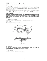
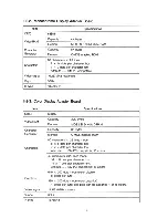
Page 4: ...PART I INTRODUCTION CONTENTS 1 1 General 3 1 2 Features 3 1 3 Description of the Computer 4 ...

Page 5: ......

Page 6: ... screen Built in Interfaces In order to input or output data to from the A 200 it has useful devices such as 5 1 4 floppy disk drive Model M1 and C1 has one disk drive and Model M2 and Model C2 has two drives RS 232C interface and printer interface Expandability In addition to the standard features listed above a customer can expand the functions of the A 200 by adding the 8087 Numeric Data Coproc...

Page 7: ...nitialize the computer when it has hang up caused by improper user s program or some machine language programs Whenever this button is pressed the computer will begin to execute the self diagnostic tests and then re Ioads the DOS or other system disk to initialize the system Keyboard Connection Jack To connect a coiled cable with a plug from the keyboard unit into this jack Keyboard To utilize whe...

Page 8: ...nal computer or serial printer Printer Connector To print out data information or programs connect a printer cable to this connector jJ Expansion 1 0 Slots The Canon A 200 can expand its functions by plugging in optional expansion cards into these expansion slots Composite Signal Jack This RCA type jack has been provided for the color display adapter board only Connect it to a composite signal inp...

Page 9: ......

Page 10: ...11 1 Product Outline 9 11 1 1 System Configuration 9 11 2 Specifications 9 11 2 1 General 9 11 2 2 Monochrome Display Adapter Board 10 11 2 3 Color Display Adapter Board 10 11 2 4 Floppy Disk Drive MDD 211 11 11 2 5 Keyboard Unit 12 7 ...

Page 11: ......

Page 12: ...or 8086 CPU Clock 4 77MHz Interrupt Eight types Main Memory Capacity Element 256K bytes with a parity bit MOS LSI 64K bit D RAM f 25b e f fhC oN 2 side double density standard track 5 1 4 Type Thin type FDD Capacity 360K bytes drive Formatted Format IBM format RS 232C type one port on the main board Serial Interface 110 9 600 baud programmable Connector pin assignment IBM PC compatible Centronics ...

Page 13: ...fications CRTC 68B45 Capacity 32K bytes Video RAM Element MOS LSI 64K bit O RAM Capacity 8K bytes Character Generator Element C MOS masked ROM 80 characters x 25 lines mode 8 x 8 dots per character box 7 x 7 dots per character font Characters Attribute IBM PC compatible 16 colors 40 characters x 25 lines mode 16 x 8 dots per character box 14 x 7 dots per character font Attribute IBM PC compatible ...

Page 14: ...e Total 327 68K bytes Formatted Capacity Per track 6 25K bytes Number of Tracks 80 Number of Sectors 16 Recording Density 5876 BPI Data transfer Rate 250K bits per second Between tracks 6 mS Access Time Seek settling 20 mS Revolution waiting 100 mS Error Rate 10 12 per bit 10 6 per seek Power Consumption 5V OAA max 12V 1 0A max 11 ...

Page 15: ...11 2 5 Keyboard Unit Item Specifications Processor 8 bit one chip microprocessor 8048 or 8748 Number of 83 keys Keys Weight Approximately 1 6kg Key Layout USA ASCII Figure 2 1 UK Figure 2 2 12 ...

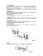
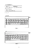
Page 16: ...GERMAN EJ 3 EJ Figure 2 3 FRENCH Figure 2 4 13 ...

Page 17: ......

Page 18: ...PART III DISASSEMBLY PROCEDURE CONTENTS 111 1 Disassembly Procedure 17 111 1 1 Top Cover 17 111 1 2 Power Unit 17 111 1 3 Main P C B 19 111 1 4 Floppy Disk Drive Unit 20 111 1 5 Keyboard Unit 21 15 ...

Page 19: ......

Page 20: ...fits the head of screws or you may damage the head 111 1 1 Top Cover 1 Remove four screws from both sides of the top cover 2 Lift the rear of the top cover and move it backward Tabs Figure 3 1 111 1 2 Power Unit 1 Unplug the AC power cords from the inlet and outlet located on the rear of the computer AC outlet tOol 0 0 10 0110 J0 I AC inlet Figure 3 2 17 ...

Page 21: ...y disk drives Power Supply Connectors Figure 3 3 3 Disconnect the cable from the power switch In this case push the tab A on the connector and pull away the connector 8 A Figure 3 4 4 Loosen the screw A and remove the screw 8 A PIS UNIT B Figure 3 5 18 ...

Page 22: ... switch cable Push this tab Figure 3 7 111 1 3 Main p e B 1 Remove the top cover 2 Remove the power unit 3 If any optional board such as display adapter or RAM board is inserted into the optional slots remove that board 4 Remove cables from the speaker keyboard connector RESET switch floppy disk drives and the cooling fan Screw Cooling Fan Connector FDD Signal Connector Keyboard Connector RESET Sw...

Page 23: ... Connector Figure 3 10 1 Disconnect the signal and power cables from the FDD Floppy Disk Drive On the body of the A drive FDD the ground wire is secured Disconnect it by removing the screw Mounting Bracket Figure 3 11 2 FDDs are mounted on the bracket Remove two screws securing that bracket to the chassis 3 Lift the bracket with FDDs away from the chassis In this case be careful not to touch inter...

Page 24: ...case by lifting it slightly and then remove both side of it Be care ful not to snap off the tabs of the bottom case 3 Pull the top case toward you slightly to free it Figure 3 12 4 Remove the screw scuring the ground wire to the keyboard base 5 Lift the keyboard with the P C B and coiled cable Figure 3 13 21 ...

Page 25: ......

Page 26: ...nnection to Peripherals 26 IV 2 4 Adjustment of Typing Angle 27 IV 3 Options 28 IV 3 1 Expansion RAM Board 28 IV 3 2 Color Display Adapter Board 28 IV 3 3 NDC 8087 29 IV 4 Summary of DIP Switch Setting 30 IV 4 1 Main Board 30 IV 4 2 DIP Switch Settings at Our Factory 32 IV 4 3 Optional RAM Board 33 IV 5 Adding Optional Floppy Disk Drive 34 23 ...

Page 27: ......

Page 28: ...IV 1 Unpacking Open the package and take out the A 200 Personal Computer Figure 4 1 25 ...

Page 29: ...r panel of the unit In order to avoid an electric shock be sure to insert the cord into this inlet first Then plug the cord into a wall outlet Figure 4 3 IV 2 3 Connection to Peripherals Referring to an instruction manual supplied with your peripherals connect them to the A 200 correctly Following illustrations on connecting display monitors show connections with the Canon A 2001 monochrome monito...

Page 30: ...11111 III n o Color Monitor Connection 01 mmmru loc Jol lillllllllill Printer Cable Printer Connection Figure 4 4 IV 2 4 Adjustment of Typing Angle The keyboard can be tilted for user s typing comfort Raise the legs located at the both corner on the bottom of the keyboard unit to tilt the keyboard Figure 4 5 27 ...

Page 31: ...city Followings are the description concerning installation for our memory expansion board Caution Before installing the memory board be sure to turn the power of the computer off and to unplug the AC power cord from the outlet Insert the connectors of the expansion board into the option slot on the main circuit board of the computer Make sure that two connectors on the expansion board are fully a...

Page 32: ...ith the 8086 CPU the performance of data processing will be dramatically enhanced To achieve this a special software is required Installation for this LSI is very simple The IC socket for this coprocessor is already provided adjacent to the CPU Insert the 8087 into this socket Figure 4 8 29 ...

Page 33: ...the following expression Total RAM capacity in byte 64K bytes 32K bytes For example if total 512K bytes of RAM are installed 512K 64K 14 E in hexadecimal 32K and actual settings are illustrated as follows DDDD 1 234 5 6 7 8 Figure 4 9 Note If all of these switches are set to OFF position the software automatically searches the actual amount of RAM installed and adjust usable RAM area to that amoun...

Page 34: ...k drive DDDDDDD DDDDDDD 1 2 3 4 5 6 7 8 1 2 3 4 5 6 7 8 1 drive 2 drives Figure 4 12 S2 6 elements Bit Function 1 For RS 232C interface 2 For printer interface 3 Not used 4 For RS 232C interface 5 For printer interface 6 Not used should always be off Table 4 2 The A 200 is equipped with the RS 232C interface and the printer interface on the main P C B however an extra interface board can also be u...

Page 35: ...ory There are four versions for the A 200 in its display type and number of disk drive At the time when the computer is shipped from the factory each element bit of the DIP switches have been set as shown in the following illustrations Model M1 ON ON U 1 2 3 4 5 6 1 2 345 6 7 8 Model M2 ON U 1 234 5 6 Mode1 C1 ON UUUUU 1 2 3 456 Model C2 ON UUUUU 1 234 5 6 Figure 4 15 32 ...

Page 36: ... the DIP switch on this board Bit Usable memory area 1 40000H 5FFFFH 2 60000H 7FFFFH 3 80000H 9FFFFH 4 40000H 5FFFFH 5 60000H 7FFFFH 6 80000H 9FFFFH Table 4 3 Example 1 Usable area 40000H 7FFFFH ON U U 1 2 3 4 5 6 Figure 4 16 Example 2 Usable area 60000H 9FFFFH ON u u 1 2 3 4 5 6 Figure 4 17 33 ...

Page 37: ...om the bracket by removing the nylon binder Nylon binder Figure 4 19 3 Disconnect the signal cables with connector from the main P C S To disconnect rotate the two hooks outwards Figure 4 20 4 Remove the FDD with bracket by referring to the paragraph Floppy Disk Drive Removal 5 Remove the hook of the clamper for the additional signal cables through the hole of the bracket In this case apply force ...

Page 38: ...4 22 7 Disconnect the plug of the drive selector on the additional FDD and reinsert it into S2 pins This defines it as the Drive 8 FDD Figure 4 23 8 Turn the mounting bracket upside down and secure the optional FDD with four screws Additional FDD Figure 4 24 35 ...

Page 39: ...nserted into the holes on the front of the chassis 10 Secure the bracket to the chassis using two screws 11 Insert the connector of the signal cables into the connector on the main P C B Index Figure 4 25 12 Connect the signal cables and power cables to both FDDs Signal cable Power cables Figure 4 26 36 ...

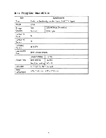
Page 40: ...PART V ADJUSTMENT CONTENTS V 1 System Clock 39 V 2 5V Power Supply 39 37 ...

Page 41: ......

Page 42: ... 244 LS04 I r SED94 20COB e LS 155 I lS20 v RAB 13 765 I LSI3B I ao 2lS I74 lS 32 B5 2LSI74 I J JV I r J 8 740 I 5 LSQ I JV I r u L 14 JV I r JV I r PI 3 CNI5 ar 33 R45 N U l N E 34 2 MADE IN JAPAN Figure 5 1 V 2 5V Power Supply 1 Connect the DC voltmeter to pin 5 or 6 RED of CN9 on the Main P C B 2 Adjust VR1 on the power supply P C B to read 5V O 05V on the DC voltmeter iI Figure 5 2 39 ...

Page 43: ......

Page 44: ...ding Circuit 57 VI 2 7 System Bus 60 VI 2 8 DMAC 63 VI 2 9 Printer Interface Circuit 66 VI 2 10 RS 232C Interface Circuit 68 VI 2 11 Timer and Speaker Driver Circuit 70 VI 2 12 Keyboard Interface 71 VI 2 13 PPI 73 VI 2 14 FDD Interface Circuit 75 VI 3 Keyboard Unit 80 VI 4 Display Adapter Boards 86 VI 4 1 Pin Description of the 68B45 86 VI 4 2 Monochrome Display Adapter Board 87 VI 4 3 Color Displ...

Page 45: ......

Page 46: ...M 16K byte ROM which contains the power on diagnostic program BIOS and IPL initial program load er the printer interface asynchronous communication interface keyboard interface floppy disk drive interface Another various control circuits are also equipped with the computer in order to work these elements effectively The power supply unit outputs three different power sources 5V B SA 12V2 0A and 12...

Page 47: ...type jack which outputs video composite signal The A 200 is equipped with one or two Canon MDD 211 5 1 4 floppy disk drive s Please refer to separate MDD 221 211 WORKSHOP MANUAL SY8 0031 721 for any further information on this disk drive The keyboard can be connected to the main unit by means of a 5 pin DIN type connector with a coiled cable The 8048 one chip microprocessor is mounted on the inter...

Page 48: ...roller 8259 Accepts interrupt signals from the I O devices and gives priority to one of them The interrupt signal selected by the 8259 is sent to the CPU PPI Programmable Peripheral Interface 8255 It has three sets of 8 bit input output ports and accesses data input from the keyboard or data set by the DIP switches UART Universal Asynchronous ReceiverlTransmitter 8250 Controls the RS 232C interfac...

Page 49: ...tem memory So 64K bit x 32 peaces 2048K bits 256K bytes of storage capacity are available Above LSls are connected to the address bus data bus and control bus so as to synchronize their functions effectively and are controlled by the CPU directly or indirectly At the same time the signals through these buses are sent to the optional slots and control the monochrome or color display adapter board o...

Page 50: ......

Page 51: ...5 A17 S4 A16 S3 Address Status outputs in three states These lines output upper 4 bits of data in memory accessing during the period of T1 When I O operation these lines are all lOW During T2 T3 TW and T4 in memory access or I O control operation a status information is output The status of the interrupt enable flag 1F S5 is reset with the beginning of each ClK cycle T1 S6 is always zero A17 S4 A1...

Page 52: ...truction in order for the CPU to determine whether the interrupt acknowledge operation is performed or not One subroutine is assigned through one interrupt vector lookup table which is located on the system memory The INTR signal can be internally masked by resetting the interrupt enable flag IF with the soft ware This signal is active HIGH NMI Non Maskable Interrupt input The NMI signal is an edg...

Page 53: ...orts 0 1 1 Halt 1 0 0 Code access 1 0 1 Read memory 1 0 Write memory 1 Passive These status signals become active during the period of T4 T1 and T2 and return to passive 111 condition during TW These signals are used by the BCU to generate all the memory and I O signals A change of S2 S1 and SO at the period of T4 is used to indicate the beginning of the bus cycle and a pas sive state of the bus a...

Page 54: ...rd interface The OSC signal is 14 31818MHz clock and sent to the monochrome board or color board through the option slots The READY signal indicates that one instruction cycle of the CPU has been completed This sig nal is made from the AEN1 and RDY1 signals The READY signal is cleared after the guaranteed hold time to the CPU has been met DClK is made from the OSC and ClK signals and used as a clo...

Page 55: ... FDC J tPD 65 Low IRO Interrupt from the printer interface Table 6 1 As Figure 6 6 shows the NMI signal is ANDed with the NMIEN signal before it is sent to the CPU This NMIEN signal is the output of the register which is assigned with the I O address OAXH from the CPU The NMIEN signal is reset when the power for the computer is turned on and when the RAM checking involved in the initial power on d...

Page 56: ... added to either one byte of even or odd address Since the A 200 uses the 4864 type dynamic RAMs everyone chip correspands to every ane bit af data bus V RAM used in the color board is 48416 type dynamic RAMs Everyone RAM chip is assigned with every 4 bits of the data bus As for the monochrome board it uses 6116 type static RAMs as V RAM Everyone chip of RAMs corresponds to one byte of even addres...

Page 57: ... operation to the even addresses the AO becomes LOW the BHE also becomes LOW and as a result both the ROMEV and ROMOD signals are output When the ROMEV is LOW the CPU selects the ROM U53 and when the ROMOD is LOW selects U62 ROM A19 A 18 1 L r _ _ A17 _ J _ I MDO 7 A16 A15 A 14 1 AO MD8 15 BHE MR D N d O E Figure 6 8 RAM Addressing The 36 D RAMs installed in the A 200 are categorized into followin...

Page 58: ...eceives this signal it sets the CPU in WAIT mode and then makes DACKO to LOW Then U97 and U90 generate RAMLE RAMLO RAMHE and RAMHO signals from the MRD signal inverted the MRD N signal output from DMAC and the inverted signal of DACKO Finally DMAC outputs refresh addresses of AO to A7 to the address bus as row addresses In this case since U47 Row Column address selector has already selected the ro...

Page 59: ...d addresses to their A through H terminals and finally gets respective even parities MDEIP MDOIP before writing data to RAMs When reading U30 and U41 input data MOO through MD7 for odd addresses and M08 through MD15 for even addresses read from RAMs into their A through H terminals and input the parity bit MDEOP for even address and MDOOP for odd address into I terminal to ensure that read data is...

Page 60: ...ignal for the 1 0 devices existing on the 110 ad dresses 000 to OFF and U117 generates the chip enable signal for the 110 devices existing on the 1 0 addresses 360 to 3FF Table 6 2 shows the schema of 1 0 map A2 113 FOC J 127 G1 Y7 f I Y6f A9 Ul17 Y5 f A8 1 G28 Y4p A6 G2A Y3 UART A5 C Y2 p A7 8 Y1 A3 A YO P 107 D Q NMIEN 87 IOW N NMIC C J 84 R RESET Gl Y7 P d 84 f U51 Y6 f Y5 p G2B Y4 G2A Y3 PPI C...

Page 61: ...inter flip flop 0000 Master clear OOOE Clear mask register OOOF All mask register bit 0020 ICW1 ICW2 OCW3 U 0021 a ICW2 ICW3 ICW4 OCW1 0040 Counter 0 load 0041 Counter 1 load f a 0042 Counter 2 load 0043 Control word 0060 Port A 0061 Port 8 a a 0062 Port C 0063 Control word READ CHO current address CHO current word count CH1 current address CH1 current word count CH2 current address CH2 current wo...

Page 62: ... Data register 68B45 data register 0 0 om 03B8 S CRT control port x 038A x CRT status port 03D4 68845 index register x 03D5 68845 data register 68845 data register 0308 Mode control register x 0 0 _m 0309 00 Color select register x Oil 03DA x Status resister 0308 Reset light pen latch x 03DC Set light pen latch x 03FO FDD control register x 0 03F4 0 Command register Status register LL 03F5 Data re...

Page 63: ...nstructions however it can access to a memory board or optional board designed for the IBM PC that are constructed with 8 bit bus Figure 6 12 shows the bus construction IW I f I Z 0 0 I I J at L 0 f I u 0 1r I I I 0 Q r I I u fi 1r I I f lr J I u 0 I I w Q f l I I f 0 I I C 0 0 0 a w L l I J rs Cl D 0 0 1 I I I I I g TI I I It C I 0 I I l I I on 0 I I 1 r l t c a C C Ow 0 3 g is uu C O C O 00 1 Z ...

Page 64: ... the direction terminals of these ICs are connected to the DEN and the T R terminals of the BCU Therefore when the CPU assigns the AO through A15 as data bus these buffers become enable When accessing on board RAM or ROM data bus is connected to these memories through U35 and U46 The reason of this is as follows since RAMs and ROMs mounted on the main board have 16 bit bus construction one byte da...

Page 65: ...mory and or 08 015 Inhibited when accessing 16 bit board memory U6 main memory and or 16 bit board memory Data buffer Accesses even addresses of Inhibited DO 07 16 bit board U68 Data buffer Accesses odd addresses of Reads writes main memory 08 015 16 bit board and or 16 bit board memory U65 Table 6 3 Signal Description MRD Memory read command MWR Memory write command lOR I O read command lOW I O w...

Page 66: ...es the HOLDA signal The HOLDA signal tells the DMAC that the CPU will insert TW signal between T3 and T4 While a signal delayed for a half clock cycle at U108 becomes the AEN signal and an inverted signal of it AEN is sent to the CEN terminal of the BCU and finally it makes the BCU inactive The AEN signal is then delayed for one clock cycle at U108 and becomes lOW level RDY signal This signal make...

Page 67: ...II II I ___ ClK DMA ClK DClK SO S2 HRQ DMAC ___ 1 DMA GO HOLDA DMAC _ _ _ _ _ _ _ _ AEN AEN BCU CEN m RDY1 DMA ADDR DACK MRD MWR __ r lOR lOW BCU MRD lOR __________________________Jl DMAC lOW MWR ______________________________ r__ I DMAC DMA RDY DMAC DMA CYCLE Figure 6 14 ...

Page 68: ...52 LOCK HRQ DMAC DMA GO HOLDA DMAC AEN AEN BCU CEN J J1 RDY1 CG MRD row RAS T4 l ____________________________________________________________ I ___ J _ _ _ _ _ _ _ _ _ _ _ _ _ _ m _ DMAC CPU _I D 1 REFRESH DMA REFRESH Figure 6 15 ...

Page 69: ...s and buffers When the CPU assigns addresses 378 through 37FH as 1 0 addresses a LOW level PTR signal is sent to U11 D U110 then makes each latch and buffer enable by decoding AD A1 10W N and 10R N signals Table 6 5 shows the definition for data bus at each 1 0 address Figure 6 17 shows the timing chart at printing Print Data 0 7 Latch SEL INIT AUTO STB ERROR SLCT PE ACK AO 1A BUSY A1 tB U110 IOW ...

Page 70: ... 379 04 05 06 07 1 0 Address Data DO 01 02 03 37A 04 05 06 07 0 51 S MIN WRITE U42 Printer Data 0 LSB Printer Data 7 MSB READ U64 Error Select Paper Empty Acknowledge Busy WRITE U49 STB AUTO FEED INITIALIZE SELECT 67 Figure 6 17 READ U138 Printer Data 0 LSB Printer Data 7 MSB Table 6 5 READ U139 STB AUTO INIT SEL ...

Page 71: ...mplete status of the UART at any time during the functional operation Status information reported includes the type and condition of the transfer operations being per formed by the UART as well as any error conditions parity overrun framing or break interrupt The UART includes a programmable baud generator Also included in the UART is a complete MODEM control capability and a processor interrupt s...

Page 72: ...ation Baud generation DC to 56k baud False start bit detection Complete status reporting capabilities When the CPU assigns one of addresses 3F8 through 3FFH as I O address the LOW level UART signal from the I O address decoding circuit is sent to the UART The UART then selects the inter nal register to be connected to the data bus according to the status of AD through A2 terminal and RD and WR ter...

Page 73: ...ls QUTO QUT1 and QUT2 respectively The QUTO terminal sends an interruption signal to the CPU through the PIC when the predeter mined timer counting has been completed The QUT1 terminal outputs a refresh request signal to the DMAC at every 15 micro seconds This signal is latched by U87 and is reset by an acknowledgement signal DACKO sent from the DMAC The QUT2 terminal generates an audio frequency ...

Page 74: ...s the start bit HIGH level which denotes that an 8 bit data will follow it This data will then be sent to the SL Shift Left terminal of the shift register U94 As for the KCLK signal it is not only converted through two stages of flip flop but also synchronized with the clock signal inside the main PC B PCLK In this case since a cycle of the KCLK is approximately 100 micro seconds while a cycle of ...

Page 75: ...U123 When the one chip microproces sor in the keyboard unit detects this LOW level signal it performs the soft reset When the soft reset signal is sent to the keyboard unit the microprocessor in the keyboard will begin to execute the self diagnostic program and then sends 1 byte return code to the keyboard interface On the main P C B the RESET signal is connected to the keyboard connector through ...

Page 76: ...7 1 0 PB7 L I Key Data LSB I Key Data LSB I Key Data LSB I Key Data LSB I Key Data LSB I Key Data LSB I Key Data LSB I Key Data LSB 0 PIT G2 terminal 0 Speaker data 0 Not used 0 Not used Description PB7 H IPL 5 1 4 disk drive 8087 installed System Memory Size System Memory Size Display Type Display Type Number of disk drive Number of disk drive 0 System Memory Parity Enable 0 Optional Memory Parit...

Page 77: ...r and when HIGH the later For more detailed information concerning the DIP switches refer to Summary of DIP Switch Setting in Part IV of this manual PPI OIP Sw1 Interrupt PC7 Control Circuit PC6 PIT OUT2 PC5 NC PC4 PC3 PC2 PC1 PCO K B Interface 07 06 PB6 05 PB5 Interrupt Control D4 PB4 Circuit D3 PB3 NC 02 PB2 NC 01 PB1 To 70 Speaker Oriver 00 PBO PIT G2 AO or BAO AO A 1 or BA1 A1 10R N RO 10W N W...

Page 78: ...EQ signal to the DMAC when data transfer to from the FOO becomes enable This signal is delayed for the time equivalent to four 2MHz clock cycles 2 micro seconds and then sent to the DREQ2 terminal of the DMAC after it is ANDed with the bit 3 of the FOD control register When the OMAC receives the DMA request it makes the CPU wait and then sends the OACK2 signal to the FOC to begin the DMA transferr...

Page 79: ...ode when HIGH FM mode LOW SYNC 0 Determines an operation mode of the VFO circuit Permits reading when HIGH inhibits LOW RW SEEK 0 Selects the functions of a signal used as both read write and seek RW when LOW SEEK when HIGH SIDE 0 Select head 0 or head 1 when dual sided drive is used LOW for head 0 HIGH for head 1 LCT DIR 0 When RW SEEK signal is in RW mode this becomes LCT and indicates that the ...

Page 80: ...the drive to write data WCLK I A timing signal for data to be written by the drive 8MHz operation FM 500kHz MFM 1MHz 4MHz operation FM 250kHz MFM 500 kHz PSO 1 0 When writing in MFM mode this determines whether the transfer speed of written data is to be advanced or delayed for obtaining a margin in load operation of the drive RDATA I Read data from the drive Consists of clock bit and data bit WIN...

Page 81: ...C 3D 30 4D_ 40 ClR DRE02 DMAC DACK I I J l14 r 113 DACK2 Figure 6 23 Pre Compensation Circuit This circuit advances or delays write data for 125 nano seconds sent from the FOC to the FOO according to the data pattern The FOC changes the status of the PSO and PS1 terminals in re sponse to a pattern of the write data sent from the CPU PSO PS1 L L Normal L H Late H L Early 78 ...

Page 82: ...1 clock cycle The SYNC signal of the FOC permits read operation at HIGH level and inhibits at LOW U126 8M ClK WO 40 40 10 10 C1 FOC 2D 20 CO Y To FDO WRITE r 30 30 C2 ClR U72 SYNC 10 PS1 B PSO A Figure 6 24 Data Separation Circuit The heart of this circuit is the VFO IC U104 SE09420COB The VFO emits the Window signal to separate data bits and clock bits from the data read from the FOO The FOC uses...

Page 83: ...status that the keyboard interface on the main PCB shows by making the key clock signal line to LOW level for 20 milli seconds Similarly the T1 terminal is used for the CPU to judge whether the buffer in the keyboard inter face on the main PCB is full or not When the buffer in the keyboard interface is full the keyboard interface will force the key data signal line to make LOW level The CPU sends ...

Page 84: ...ve been pressed In this way the CPU avoids a chattering Figure 6 28 is the timing chart when the CPU transmits key data to the main PCB First the CPU makes key data to HIGH level reads these levels at TO and T1 terminal and then checks whether the keyboard interface on the main PCB have been made this line to LOW level or not Next the CPU sends 1 bit of HIGH level data start bit to the keyboard in...

Page 85: ... ALT OF I 57 39 SPACE 16 10 Q 58 3A CAPSLOCK 17 11 W 59 3B F1 18 12 E 60 3C F2 19 13 R 61 3D F3 14 T 62 3E F4 21 15 Y 63 3F F5 22 16 U 64 40 F6 23 17 I 65 41 F7 24 18 0 66 42 F8 19 P 67 43 F9 26 1A 68 44 F10 27 1B 1J 69 45 NUM LOCK 28 1C J 70 46 SCROLL LOCK 29 10 CTRL 71 47 7 HOME 1E A 72 48 8 i 31 1F S 73 49 9 PGUP 32 20 0 74 4A 33 21 F 75 4B 4 34 22 G 76 4C 5 23 H 77 40 6 36 24 J 78 4E 37 25 K 7...

Page 86: ...LT OF I I 57 39 SPACE 16 10 Q 58 3A CAPSLOCK 17 11 W 59 3B F1 18 12 E 60 3C F2 19 13 R 61 3D F3 14 T 62 3E F4 21 15 Y 63 3F F5 22 16 U 64 40 F6 23 17 I 65 41 F7 24 18 0 66 42 F8 19 P 67 43 F9 26 1A 68 44 F10 27 18 1 J 69 45 NUM LOCK 28 1C 70 46 SCROLL LOCK 29 1D CTRL 71 47 7 HOME 1E A 72 48 8 i 31 1F S 73 49 9 PGUP 32 20 0 74 4A 33 21 F 75 4B 4 34 22 G 76 4C 5 23 H 77 40 6 36 24 J 78 4E 37 25 K 79...

Page 87: ...38 ALT OF I 57 39 SPACE 16 10 Q 58 3A CAPSLOCK 17 11 W 59 3B F1 18 12 E 60 3C F2 19 13 R 61 3D F3 14 T 62 3E F4 21 15 Z 63 3F F5 22 16 U 64 40 F6 23 17 I 65 41 F7 24 18 0 66 42 F8 19 P 67 43 F9 26 1A 0 68 44 F10 27 1B 69 45 NUM LOCK 28 1C 70 46 SCROLL LOCK 29 10 CTRL 71 47 7 HOME 1E A 72 48 8 i 31 1F S 73 49 9 PGUP 32 20 0 74 4A 33 21 F 75 4B 4 34 22 G 76 4C 5 23 H 77 40 6 36 24 J 78 4E 37 25 K 79...

Page 88: ...6 38 ALT OF 1 I 57 39 SPACE 16 10 A 58 3A CAPSLOCK 17 11 Z 59 3B F1 18 12 E 60 3C F2 19 13 R 61 3D F3 14 T 62 3E F4 21 15 Y 63 3F F5 22 16 U 64 40 F6 23 17 I 65 41 F7 24 18 0 66 42 F8 19 P 67 43 F9 26 1A 68 44 F10 27 18 69 45 NUM LOCK 28 1C 70 46 SCROLL LOCK 29 1D CTRL 71 47 7 HOME 1E Q 72 48 8 i 31 1F S 73 49 9 PGUP 32 20 D 74 4A 33 21 F 75 4B 4 34 22 G 76 4C 5 23 H 77 4D 6 36 24 J 78 4E 37 25 K ...

Page 89: ...ut puts turns three state buffer Unless the CPU reads the contents of the register of the CRTC this bus remains high impedance RIW ReadIWrite This signal controls a direction of data transferring between the CRTC and the CPU That is when this signal is HIGH a data from the CRTC is transferred to the CPU and when LOW a data from the CPU is transferred to the CRTC CS Chip Select Only when the CS sig...

Page 90: ...c signals MAO MA13 Refresh Memory Address These signals are memory address outputs for refreshing an information on the CRT at certain period of time As for the color display adaptor board the CRTC supports 8 display pages RAO RA4 Raster Address This signal is a raster select signal for the character generator CUDISP Cursor Display This video signal is used for displaying a cursor sign on the CRT ...

Page 91: ... A_Y f L L t A B L 0 0 68B45 DO MAO I I 07 MAIO RAO I RA3 ATO AT7 1 00 AO t I I AIO 1 07 L RAO RA3 ATO AT7 0 0 Tt 0 0 I Attribute Generator L t II Video Output Generator VIDEO Output INTENSITY Output HSYNC Output VSYNC Output Clock Generator I I AE 10 lOW Decoder r t r 0 0 T 0 CURSOR HSYNC VSYNC OISPEN 0 j4 V A I L 0 0 MRD MWR 0 0 T Y V RAM RIW I Control Figure 6 30 ...

Page 92: ...lustrated as follows 7 6 5 4 3 2 0 Character Code Even Address Attribute Code Odd Address 1 L Foreground Intensity T L _ _ _ _ _ _ _ _ _ _ Background Blink Background Foreground Display mode R G B R G B 0 0 0 0 0 0 Non display 0 0 0 0 0 1 With underline 0 0 0 1 1 1 Normal display 1 1 1 0 0 0 Reverse display Table 6 12 Blink Display mode Intensity Display mode 0 Non blink 0 Normal intensity 1 Blink...

Page 93: ...tion 3B4 68B45 Index register 3B5 68B45 Data register 3B8 CRT Control port 3BA CRT Status port Table 6 14 Further 3B8 and 3BA are assigned as follows 1 0 Address Bit Description 3B8 0 High resolution mode 3 Video enable 6 Blink enable Table 6 15 Unless the address 3B8 is 01 OSC signal in not output and as a result nothing is displayed on the screen I O Address Bit Description 3BA 0 H sync 3 B W vi...

Page 94: ...l clock signal for control ling the display adapter itself and a display monitor 5V 5V b WE F r C S 0 WE 5 A OA 10 B OB 15 D R 1 4 C OC J Jv D OD U4 lS161 CRTC ClK 14 5V ET CY s I L EP r ClK lOAD 1 20 p CPU CRTC ClK Figure 6 31 OSC OA 08 OC OD s c CRTC ClK CPU CRTC 08 OC WE F_ _ _ I WE Figure 6 32 91 ...

Page 95: ...gnal to be sent to the D terminal is made by NANDing the EX ORed output of OB and OA and the CRTC CLK signal This WE Signal becomes the writing signal to the V RAM when the CPU cycle Attribute Generator Figure 6 33 is an overview of this circuit Descriptions for each output signal is as follows NON DISP This signal is made by decoding the attribute signals That is when the ATO AT1 AT2 AT4 AT5 and ...

Page 96: ...E 2D 20 J 15 1 UNDER LINE 12 3D 30 U27 lS139 AT4 ClK G I YO ClR AT5 A AT6 B U24 3Pin 12 U8 lS139 7 L o G n A B Y3 I OSC S I L U8 lS139 RA2 YO r G RA3 11 I 5V RAO A RA1 B AT7 U2 lS393 U2 lS393 RESET ClR ClR V SYNC A OD A QA BLINK 11 BLINK EN CURSCR CURSOR CURSOR Figure 6 33 93 ...

Page 97: ... is ORed with the UNDERLINE signal Namely when either the character signal or the UNDERLINE signal is HIGH the pin 6 of U7 becomes HIGH_ Next the output of 6 pin is ANDed with the NON DISP signal and the BLINK signal by U28_ In this case either one of these two signals is LOW the output terminal of U28 12 pin becomes LOW Then this output signal is ORed with the CURSOR signal by U7 Finally the outp...

Page 98: ...e pin 8 of U1 is HIGH and when this signal is accessing the V RAM in the CPU cycle the OE signal of the 6116 then becomes LOW 3 Next a data is output from the 6116 This data is latched at the rising edge of the 1 0 READY signal and simultaneously it makes the 1 0 READY signal enable 4 The CPU then reads the data which has been latched at the falling edge of the T4 cycle 5 When the CPU enters into ...

Page 99: ...61 5n OSC T2 T3 Tw Tw Tw T4 CPU ClK II r l r l r l r l II I CRTC ClK r S I it 6116ADR CPU CPU CFfFc CPU CRTC CPU _ x CRTC co 0 MRD I O READY Ul PIN 8 61160E 6116 DATA DATA CPU DOUT CPU Figure 6 35 ...

Page 100: ...ignal In this case if the pin 5 of U5 is HIGH and the CPU is in memory write mode the OE signal of the 6116 becomes lOW Then the data sent from the CPU is written to the 6116 3 The 1 0 READY signal becomes HIGH at the rising edge of the CRTC ClK signal When the CPU cycle is changed from TW cycle to T4 cycle the MWR signal becomes HIGH Then an impedance of the I O READY signal becomes high 97 ...

Page 101: ...OSC T2 CPU ClK CRTC ClK I I j I I I J sf U5 5PIN I I I I I I I I 6116 ADR J CPU X CRTC X CPU X CRTC X CPU X CRTC X CPU X CRTC CO Xl MWR I I r I O READY I I I Ul 8 PIN 6116WE 6116 DATA I Figure 6 36 ...

Page 102: ...2364 Since the 2364 can always be accessed it output a data on to the data bus when the address is determined This data is input to the shift register LS166 when the S L signal is LOW and is output at the next OSC clock after it is shifted corresponding to everyone pixel on the screen As well as the CH Character signal the AT Attribute signal is output when in the CRTC mode A data output from the ...

Page 103: ... 61 5n OSC CRTC CLK CPU CRTC sf 6116ADDR v CPU x CRTC Tx CPU CRTC CPU CRTe 61160E 0 61161 00 1107 DOUT 0 2364 ADDR ROM ADDR ROMA ROM ADDR DATA OUT DATA OUT 2364 DATA QH AT AT VIDEO OUT Figure 6 37 ...

Page 104: ...25 or 40 x 25 characters in one screen 8 x 8 pixels for one character box 7 x 7 pixels for one character With character attribute Can display 256 different characters Video signal 14 31818MHz maximum V sync signal 60Hz H sync signal 15 75kHz I g r 1 w 3 1 I If I u u 8 0 z z e r I to r t L I I o 0 T N o I x J r 8 I M I I e 0 2 2 f J r 0 0 e I o l B E 11 a 5 I I ex r t j 8 rl u I 0 1 1 1 II II LI L ...

Page 105: ... byte are illustrated as follows 7 6 5 4 3 2 1 0 C1 CO C1 CO C1 CO C1 CO First display element Second display element Third displa element y Fourth disp element lay Table 6 17 Colors to be dispalyed are selected with CO and C1 above The color selection is done by the IC U19 LS174 640 x 200 Pixels Graphics Mode In this high resolution mode every bit of the V RAM corresponds every pixel on the scree...

Page 106: ...e 16K bytes 640 x 200 pixels graphics mode 16K bytes Clock Generator Circuit This circuit that is illustrated in the figure below generates a fundamental clock signal for control ling the display adaptor itself and a display monitor Detailed description for every clock signal is as follows u u I a 0 I u u 0 J 1 1 N 0 0 M N 1 1 in CD CD M M N N r co M J l J 0 M J col co r I N M M N f M I vOl CD 0 c...

Page 107: ... output and an NORed signal of U18 2 pin output and U66 5 pin output are ORed at U58 and this signal is used as the SIC sig nal For 640 x 200 pixels screen the cycle of the S L signal is extended to a double and used as the lOAD signal of the shift register which shifts the dot data in the graphics mode CAS This signal is an ANDed signal of U64 2 pin output and U60 6 pin output This clock is used ...

Page 108: ...is selected by the U5 and then sent to the U49 9 pin Further the signal from U57 4 pin is input to both U33 14 pin and U34 14 pin These two ICs add an information concerning an attribute to the character data and then output to U32 which synchronizes these outputs with the DOT ClK signal a co CD CD N t 0 0 01 eX t 0 0 0 Ol W I I J t M 01 j l en U t J I leI 1 01 0 0 0 1 IVl t M 01 91dM M M 01 CD t ...

Page 109: ... I I 02 I I 03 I II I II 7M I I I I I I I II I I I I I I I I 0 m 3 58M I I I II I I I CAS CC I I I I I lClK CRTC CLK 1 I II HClK I I J RAS J I I I IJ CAS J I I I I I I I I I S L HIGH J I I I I S L I I LOW DOT ClK COLOR CRT CLOCK GENERATOR TIMING Figure 6 41 ...

Page 110: ... r CRTC RAS ADDR CRTC CAS ADDR CRTC ADDR COLUMN ROW COLUMN ROW COLUMN IROWX _ _ _ CH lATCH AT lATCH 0 sf J DOT ClK 14MHz I lATCH DATA CLEAR DISP DISP CRTC ADDR CRTC o lATCH ADDR MA O MA l 80 x 25 CHARACTERS TEXT MODE TIMING Figure 6 42 ...

Page 111: ... I I I I J I I II ROW I I X 1 COLUMN CRTC RAS ADDR I I CRTC CAS ADDR I I o to CRTC ADDR CH lATCH AT lATCH CRT ClK sf DOT ClK 7MHz J J I I I I I I I ROW I I X I I I COLUMN I I I I I I I I I I lATCH DATA CLEAR r DISP I DISP CRTC ADDR CRTC I X 0 y lATCH ADDR X MA O 40 x 25 CHARACTERS TEXT MODE TIMING Figure 6 43 ...

Page 112: ...LUMN I I I I I II I I 1 I I I ROW 1 1 If I I 1 X COLUMN o cc CRTC RAS ADDR CRTC CAS ADDR CRTC ADDR CH lATCH AT lATCH Q2 SIC W DOT ClK I I I I I I I I I ROW I I X I I J COLUMN I 1 f I I I I I I I I lATCH DATA CLEAR I DISP II DISP CRTC I 320 x 200 640 x 200 GRAPHIC MODE TIMING Figure 6 44 ...

Page 113: ...nt when the ROM address is decided a data is output from the character generator 2364 This data is input to the shift register U25 lS166 together with the S l signal and shifted per one bit This CH data is mixed with the AT data and then latched to output Note that the cycle of the fundamental clock signals DOT ClK CH lATCH AT lATCH SIC are different in both display mode 110 ...

Page 114: ...I SLJl JlJLn SlILfU1 J1 JUlSru u u u u u uLnJLn JL CH lATCH II I I I I I I I I AT lATCH I I I I CH DATA X ROM ADORESS ROM DATA X X X x AT DATA IX ATTRIBUTE DATA IX IX I IX 1 SHIFT REG lQ2AD61 D51 04X 03 X02 XD1 100 D7X06 XD5X D4I03 X02 X 01 XOO D7X06XD5 X 04 XD3X D2X 01 XDO 07 XD6X 05X D4X D3X 02X DlX 00 07X D6X 051 D4 _ I R G B I IDOX D7 106X 05 X04 X03 102 101 I DOID7X 06 ID5X 04I03XD2X 01 IDOX ...

Page 115: ...output synchronizing with the DOT ClK Signals after a color information is mixed to it As mentioned above since one dot consists of 2 bits four 22 colors can be displayed 640 x 200 Pixels Graphics Mode Basically a method of displaying for this mode is identical to the 320 x 200 pixels mode How ever since every dot to be displayed corresponds to every bit no color except black and white can be used...

Page 116: ...OSC DOT ClK CH lATCH AT LATCH S L 1 CH DATA X EVEN DATA AT DATA SHIFT REG w R G B 1 320 x 200 GRAPHIC VIDEO OUT C1 EN CO EN R G B 1 640 x 200 GRAPHIC VIDEO OUT Figure 6 46 ...

Page 117: ... V and 7 V generated by 022 and C24 The 5 V power supply has a over voltage protection circuit which is controlled by photo coupler PC1 When an over voltage is detected the photo coupler PC1 activates and then control voltage for IC1 on the sub printed board is cut off IC2 acts as an over current protector for the 5 V and 12 V power supply lines This IC detects voltage drops at R53 and R52 which a...

Page 118: ......

Page 119: ...PART VII DIAGNOSTIC PROGRAMS CONTENTS Diagnostic Programs 118 116 ...

Page 120: ......

Page 121: ...ed into the built in ROM and whenever a customer turns the com puter on or the RESET button is pressed the computer will perform this test automatically The test program checks such devices or functions as ROM RAM keyboard timer and video Following is a detailed flow chart of this test _ __ JMP FE05B Disable interrupt Disable display Initialize the DMA Page Register Initialize the PPI Disable pari...

Page 122: ...1 Set dummy stack Check the OMAC Set video interrupt vector address YES Enable parity error Check hot interrupt Initialize the DMAC YES Initialize the PIC I YES Check Timer 0 YES Check System RAM OOOOO OFFFF YES Initialize Timer 0 HALT ...

Page 123: ... high segment address XX and read data YY XXYY Display error code 201 N o Enable video Check H SYNC Execute the KEY RESET NO YES Read key data YES Display key data Check the RAM except the System RAM Display error code 301 YES 5 4 ...

Page 124: ...te FDD YES Read IPL record Check FDD seeking YES NO YES 01i t i t I r Oecriment the ilt COUI I f Display error code 601 NO Check the number of the installed RS 232C port Check the number of the installed printer port Display the following error message Non Syster n disk Replace and END ...

Page 125: ...ert the Diagnostic disk into the drive A and the computer will begin to load this program automatically Then the following message will appear Canon Personal Computer DIAGNOSTIC C Copyright Canon Inc 1984 Ver 1 0 Press any key to start Once this message appears it is indicated that the whole contents in the disk have been trans ferred into the internal RAM So in order to prevent the disk from acci...

Page 126: ... 256 KB memory If OK press Y if not press N If these items fit your computer actually press Y key and then the screen will change its indica tion to Menu Or if not press N key The A 200 will store the data temporarily into RAM and also returns to Menu MAIN MENU I AUTO CHECK 2 EACH CHECK 3 LOG 4 COPY 5 EXIT DIAGNOSTIC Select the number in this menu 1 AUTO CHECK When you choose this item following t...

Page 127: ...f an error occurs following message will appear segment XXXX Number of address where an error was occurred offset YYYY Number of address where an error was occurred write data ZZZZ Previously written data read data WWWW Read data Press any key to exit When this check is completed successfully the message Memory read write check OK Press any key to exit To exit this test Pressing any key returns th...

Page 128: ...s Press A key to check drive A Press B key to check drive B Press ESC key to exit will appear Press appropriate key in response to above prompt Error Message Disk R W error WXYYZ Press any key to return where W is a drive number X is a head number YY is a track number and Z is a sector number To exit this test After the prompt below press any key then ESC key The test will return to EACH CHECK Men...

Page 129: ...sage None You should check the information displayed on the screen with your eyes by referring to the illustrations above To exit this test When you enter Yes or No in response to the question displayed on the last screen the test will return to EACH CHECK Menu 126 ...

Page 130: ...UY WIY1 J _ bc d fQt ll J l opqr t w yl H I I 1012 45678 1 I _ IABCDEFG HIJrLI WOf OASTUYWIVl _ Hcd 1 J I opqrtit v y C 012345678 H X l 11 v 8CDEFGHIJ LI1NOPORSnJWlvlr _ bcCl f t 1 JII ot t t v yl Error Message If an error at the interface is detected one of the following messages will ap pear after the prompt TIME OUT ERROR Echo back check error 110 error Printer is not selected Out of paper Ackn...

Page 131: ...m to return to the main menu CLEAR LOG list This command clears all error data stored on the RAM and on the disk currently in use RETURN to main menu Select this command to return to Main menu 4 COPY The information stored into Diagnostic Program disk cannot be copied onto another one with the DISKCOPY command provided in the DOS because this Diagnostic Program is not con trolled by the DOS Use th...

Page 132: ...stic program and return to DOS mode A message Insert system disk in drive A Press any key to get ready will be displayed Remove Diagnostic Program disk and insert the DOS disk instead and then press any key The computer will begin to boot the DOS disk 129 ...

Page 133: ...PART VIII TROUBLESHOOTING 130 ...

Page 134: ......

Page 135: ...Troubleshooting Insert the diagnostic diskette into drive A Turn the power switch on and push the clamp button on drive A No No 7 Yes 132 ...

Page 136: ...Segment DO 01 02 03 04 05 06 07 OO OF Not checked in this test ll U36 or U31 or U26 or U22 or U18 or U13 or U9 or U5 or U1 or 10 1 F 0 a U37 U32 U27 U23 U19 U14 U10 U6 U2 c co U38 or U33 or U28 or U24 or U20 or U15 or U11 or U7 or U3 or 20 3F U39 U34 U29 U25 U21 U16 U12 U8 U4 0 U2 or U3 or U4 or U5 or U6 or U7 or U8 or U9 or U10 or co 40 5F 0 U11 U12 U13 U14 U15 U16 U17 U18 U19 m g U21 or U22 or U...

Page 137: ...e whose key switch is always on refer to Table 6 11 and replace it 301 Key Reset is not completed Check the PPI CS AO A1 RO WR and 00 07 signals Check the interface signals 97 5 260 15 KCLK Start Bit P10 P21 P22 15t data 2nd data Figure 8 2 134 ...

Page 138: ...gure 8 4 Che ck the signals shown below INDEX Pin 17 of FDC SIDE Pin 27 of FDC TRKO Pin 33 of FDC WG Pin 25 of FDC DRIVE 0 Pin 8 of U132 DIR Pin 38 of FDC DRIVE 1 Pin 6 of U132 STEP Pin 37 of FDC PIT or PIC failure An unexpected interrupt has been received during the interrupt mask register of PIC is reset or the timer 0 clock is too early or too late Check IRQO 7 and INT signals Check PCLK CLKO C...

Page 139: ... o Character Code Even Address U43 I IBli RIG I U40 B II I I RIG I B I Attribute Code Odd Address Foreground r T Intensity Background T Blink Figure 8 6 2 Color Board Check for lower 4K byte of V RAM Using the 80 x 25 characters text mode determine the error bit If the error bit is in even address the displayed character may be different and if the error bit is in odd address the displayed attri b...

Page 140: ... Check for the 16K byte V RAM Using the 320 x 200 pixels graphic mode determine the error chip U21 U20 U20 U21 U22 U23 U20 U21 U22 U23 320 Pixels Figure 8 8 200 Pixels 137 ...

Page 141: ...e H SYNC signal VIDEO I H SYNC II I I L I I O 62J 1s 8 30J ls 44 29J 1s 1 04r 54 25J 1s VIDEO I I I I V SYNCL j LJ O 32ms I I 1 I 18 99ms O 16ms O 87ms 20 00ms Figure 8 9 Check the clock generator circuit DOT ClK I _ 246 0ns _ ________________ r__ CPUlCJrn J sf J Figure 8 10 138 ...

Page 142: ... L 7 26 s J VIDEO I I I I I I V SYNC 1 71 ms I I O 19ms 12 70ms r L 2 03jS 16 67ms Figure 8 11 Check the clock generator circuit OSC 14 31818MHz DOT ClK 3 58MHz lOW CRTC ClK HIGH S HIGH RAS CAS I J I I l I J I I J I J I n I n LJ I LJ I I I n I n I I I I I I I I I LJ I I I n I L Figure 8 12 139 ...

Page 143: ...t the DC voltmeter to CN9 and check 5V 12Vand 12V Pin No Color Description 1 GRAY GND 2 GRAY GND 3 BLACK GND 4 BLACK GND 5 RED 5V 6 RED 5V 7 YELLOW 12V 8 ORANGE 12V Table 8 2 Check the CG OSC ClK PClK L DClK I L RES RESET Figure 8 13 Check the BCU T4 T1 T2 T3 T4 ClK SO S1 S2 I RD AWR INTA I WR r Figure 8 14 140 ...

Page 144: ...low Address Contents FFFFO EA5BOOOFO JMP FOOO E05B FE05B FA CLI FE05C FC CLD FE05D 8CC8 MOV AX CS FE05F 8ED8 MOV DS AX FE061 BE70EO MOV SI E070 FE064 AD LODSW FE065 3DFFFF CMP AX FFFF FE068 741D JZ E087 FE06A 8BDO MOV DX AX FE06C AC LODSB FE06D EE OUT DX AL FE06E EBF4 JMP E064 FE070 B80301 FE073 D803 FE075 008300FF FE079 63 FE07A 00996100 Table 8 3 141 ...

Page 145: ...e 8 16 Check the system RAM T2 T3 TW T4 _ CPU ClK J lC51 19P MRD IC107 3P D OUT ______ _________________________________L________ _________ _ PARITY U107 2Pin PC7 Figure 8 17 Check the DMAC CPU ClK DMA ClK HRQ HOLDA AEN 8288 RDYI 8284 Figure 8 18 142 ...

Page 146: ......

Page 147: ...er Supply P C B Assembly Diagram 160 IX 1 10 Power Supply P C B Parts 162 IX 1 11 Monochrome Display Adapter Board Assembly Diagram 163 IX 1 12 Monochrome Display Adapter Board Parts 164 IX 1 13 Color Display Adapter BoaJd Parts 166 IX 1 14 Color Display Adapter Board Parts 167 IX 1 1S RAM Board Assembly Diagram 169 IX 1 16 RAM Board Parts 170 IX 2 Circuit Diagrams 172 IX 2 1 Main Circuit 1 172 IX...

Page 148: ......

Page 149: ...000 1 KEYBOARD CONNECTION JACK 16 SY1 0811 000 1 FAN MOTOR ASSEMBLY 17 SY1 0812 000 1 SPEAKER 19 SY1 0999 000 1 FRONT COVER ASSEMBLY 20 SY1 0989 000 1 BOTTOM CASE COVER 21 1 SLOT BRACKET COVER 22 1 CENTER ARM 23 24 SY1 1084 000 1 1 FRONT PANEL REAR PANEL 25 1 BOTTOM CASE 26 1 POWER SWITCH GUARD 27 28 SY1 0991 000 1 1 FDD TOP MOUNTING COVER BRACKET 29 30 SY1 0992 000 SY1 0993 000 4 1 SLOT BRACKET F...

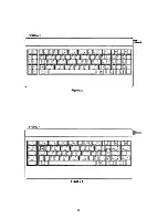
Page 150: ...8 IX 1 3 Exploded View of Keyboard II 9 3 147 ...

Page 151: ...143 104 VRl 1143 103 1 1 1 1 1 1 1 1 1 1 1 1 1 1 1 1 1 1 1 1 1 CARBON CARBON CARBON CARBON CARBON CARBON CARBON CARBON CARBON CARBON CARBON CARBON CARBON CARBON CARBON CARBON CARBON CARBON CARBON CARBON CARBON RESISTOR RESISTOR RESISTOR RESISTOR RESISTOR RESISTOR RESISTOR RESISTOR RESISTOR RESISTOR RESISTOR RESISTOR RESISTOR RESISTOR RESISTOR RESISTOR RESISTOR RESISTOR RESISTOR RESISTOR RESISTOR l...

Page 152: ... F7 8Yl 0897 000 1 KEY TOP F8 5Y1 0898 000 1 KEY TOP F9 oJ 5Yl 0899 000 1 KEY TOP FlO 5Yl 0900 000 1 KEY TOP SHIFT LEFT 5Y1 0901 000 1 KEY TOP 1 I oJ 5Y1 0902 000 5Y1 090 3 QQQ 1 1 KEY KEY TOP TOP 2 3 5Y1 0904 000 1 KEY TOP 4 8Y1 0905 000 1 KEY TOP 5 5Y1 0906 000 1 KEY TOP 6 8Y1 0907 000 1 KEY TOP 7 8Y1 0908 000 1 KEY TOP 8 8Y1 0909 000 5Y1 0910 000 8Y1 0911 000 1 1 1 KEY TOP KEY TOP KEY TOP 9 0 B...

Page 153: ...EY TOP SCROLL LOCK SY1 0930 000 1 KEY TOP SHIFT RIGHT SY1 0931 000 1 KEY TOP CAPS LOCK SY1 0932 000 1 KEY TOP ALT SY1 0933 000 1 KEY TOP INS SY1 0934 000 1 KEY TOP DEL SY1 0935 000 1 KEY TOP SPACEBAR SY1 0947 000 1 KEY TOP ESC SY1 0948 000 1 KEY TOP PRT SC 1 SY1 0802 000 1 CURL CORD ASSEMBLY 2 SY1 08S1 000 1 PANEL 3 SY1 08S2 000 1 LEVER 4 SY1 0936 000 1 GUIDE PIN FOR SPACEBAR 5 SY1 0937 000 1 GUID...

Page 154: ......

Page 155: ......

Page 156: ......

Page 157: ... SY1 0983 000 SY1 0986 000 SY1 0985 000 1 1 1 RESISTOR RESISTOR RESISTOR ARRAY ARRAY ARRAY lK OHM X 8 4 7K OHM X 8 4 7K OHM X 4 Rl0 VRl 1143 102 Rl1 VRl 1143 102 R12 VRl 1143 331 R13 VRl 1143 331 R14 VR1 1143 331 R15 VR1 1143 331 R16VR1 1143 472 R17 VRl 1143 105 R18 VRl 1143 202 R20 VR1 1143 101 R22 VR1 1143 221 R24 VR1 1143 472 R25 VRl 1143 102 R26 VR1 1143 301 R27 VR1 1143 330 R28 VR1 1143 331 R...

Page 158: ... X65 7160 000 1 U55 WA3 0320 000 1 U56 WA3 0805 000 1 U57 WA3 0361 000 1 U58 WA3 0361 000 1 U59 SY1 0849 000 1 U60 WA3 0336 000 1 U61 SY1 0835 000 1 U62 EY3 0172 000 1 63 WA3 0428 000 1 U64 WA3 0145 000 1 i DESCRIPTION REMARK CARBON RESISTOR 750K OHM 1 4W 5 CARBON RESISTOR 4 7K OHM 1 4W 5 CARBON RESISTOR 33 OHM 1 4W 5 CARBON RESISTOR 330 OHM 1 4W 5 CARBON RESISTOR 330 OHM 1 4W 5 CARBON RESISTOR 33...

Page 159: ...3 0134 000 WA3 0137 000 WA3 0289 000 X65 7160 000 WA3 0002 000 WA3 0134 000 WA3 0137 000 WA3 0135 000 WA3 0134 000 WA3 0336 000 WA3 0145 000 WA3 0135 000 Q TY 1 1 1 1 1 1 1 1 1 1 1 1 1 1 1 1 1 1 1 1 1 1 1 1 1 1 1 1 1 1 1 1 1 1 1 1 1 1 1 1 1 1 1 1 1 1 1 1 1 1 1 1 1 1 1 1 1 1 1 1 1 1 1 1 1 1 1 1 1 1 1 1 1 1 1 IC HD74LS04P use HITACHI s IC only IC MPB8284AD IC SN74LS174N IC SN74LS32N IC SN74LS174N IC...

Page 160: ...42 VC4 4254 104 1 CERAMIC CAPACITOR 0 1 MF 25V C43 VC4 4254 104 1 CERAMIC CAPACITOR 0 1 MF 25V C44 VC4 4254 104 1 CERAMIC CAPACITOR 0 1 MF 25V C45 VC4 4254 104 1 CERAMIC CAPACITOR o 1MF 25V C46 VC4 4254 104 1 CERAMIC CAPACITOR 0 1 MF 25V C47 VC4 4254 104 1 CERAMIC CAPACITOR 0 1 MF 25V C48 VC4 4254 104 1 CERAMIC CAPACITOR 0 1 MF 25V C49 VC4 4254 104 1 CERAMIC CAPACITOR 0 1 MF 25V C50 VC4 4254 104 1...

Page 161: ...lMF 25V Cl04 VC4 4254 104 1 CERAMIC CAPACITOR O lMF 25V Cl05 VC4 4254 104 1 CERAMIC CAPACITOR O lMF 25V Cl06 VC4 4254 104 1 CERAMIC CAPACITOR O lMF 25V Cl07 VC4 4254 104 1 CERAMIC CAPACITOR O lMF 25V Cl08 VC4 4254 104 1 CERAMIC CAPACITOR 0 1MF 25V Cl09 VC4 4254 104 1 CERAMIC CAPACITOR O lMF 25V Cl10 VC4 4254 104 1 CERAMIC CAPACITOR O lMF 25V Cl11 VC4 4254 104 1 CERAMIC CAPACITOR O lMF 25V Cl12 VC4...

Page 162: ...IX 1 9 Power Supply p e B Assembly Diagram 160 ...

Page 163: ...076A D28 SY1 l032 000 1 SILICON DIODE V19C 029 SY1 1033 000 1 SILICON DIODE 1SS81 ZD1 ZDl WA1 0095 000 WA1 0l10 000 ZENER ZENER DIODE DIODE HZ3Al HZ6Al ZD3 WA1 0110 000 ZENER DIODE HZ6Al ZD4 WA1 0212 000 ZENER DIODE HZ12C3 ZD12 WA1 0095 000 ZENER DIODE HZ3Al TRKl SY1 1042 000 1 THYRISTOR SMl 2G41 Ll SY1 1050 000 1 CHOKE COIL L2 SY1 1049 000 1 CHOKE COIL Tl SY1 1043 000 1 POWER TRANSFORMER FHl SY1 ...

Page 164: ......

Page 165: ......

Page 166: ......

Page 167: ......

Page 168: ......

Page 169: ......

Page 170: ......

Page 171: ......

Page 172: ...J f L 1 RS 1 __1 1 4 Z__1 _4 _ r i I R4 __1 1 1 1U114 y 60 L5DDJ Ol IOJ 1 D1tLt__ID1 __ UIZ9 L rl WA 00 f L IOO I 1 80 80J a J07 AI Io lQ 70f L J06 A11 i 60 60 _IO AI 1 _ _ iA l L SO SOr L I04 A 0 All 1 4Q o loO _IDl A 0410 JQ J orl t__J01 A A9 10 10 t IOI 8 L 10 10 I JOO A A ft A J A A A 0 lOCI CPU 8Al A AJ l A l A Y AI At lA J1V r AI 4D_LtA 1G1V AD c nf I FAN I I CH An lOP I 1104 a IM All IJ UII...

Page 173: ...0 5V U J R52 N Ji NO IM 1 U2 tj6 m 00 0 g o le3 THI RSO K TL431CLP B R32 330 r IVE J U40 C31 330 1 O 39 90 i1 026 RH 1 5K Nf u Z03 8 fG 01 0 1 t 2 a 5A CNI 5 CNI 6 CN2 4 CN3 4 CNI I CNI 2 CNI 3 CNI 4 CN2 2 CN2 3 CN3 2 U C J CJ 7 nt 1 1 1 J 0 0 I J 0 CD I OC I CD I Z P z o Il I 0 o 00 r I 02 TRI 2SAI048 Y 12 12 r SWlil J II AOPt rp tj IC I uPD49C 16 e R 6 9 1K 10K R43 330 90 R37 8 2K 1 olC iI 1141 ...

Page 174: ......

Page 175: ......

Page 176: ......

Page 177: ...82 X 1 1 RS 232C Interface 183 X 1 2 Monochrome Monitor Interface 183 X 1 3 Color Monitor Interface 183 X 1 4 Video Composite Interface 183 X 1 S Printer Interface 184 X 1 6 Option Slot Interface 186 X 1 7 Printer Cable 187 X 2 Character Code Table 189 180 ...

Page 178: ......

Page 179: ...t To Send Output 5 Clear To Send Input 6 Data Set Ready Input 7 Signal Ground 8 Carrier Detect Input 9 Not Used 10 Not Used 11 Not Used 12 Not Used 13 Not Used 14 Not Used 15 Not Used 16 Not Used 17 Not Used 18 Not Used 19 Not Used 20 Data Terminal Ready Output 21 Not Used 22 Ring Indicate Input 23 Not Used 24 Not Used 25 Not Used 1 14 25 182 13 ...

Page 180: ...put Video Output Horizontal Output Vartical Output X 1 3 Color Monitor Interface Pin No 2 3 4 5 6 7 8 9 Description Ground Ground Red Green Blue Intensity Reserved Horizontal Vartical InpuVOutput Output Output Output Output Output Output Output X 1 4 Video Composit Interface Pin No 2 Description Composit Signal Ground InpuVOutput Output 183 ...

Page 181: ...it 1 Output Data Bit 2 Output Data Bit 3 Output Data Bit 4 Output Data Bit 5 Output Data Bit 6 Output Data Bit 7 Output Acknowledge Input Busy Input Paper End Input Select Input Auto Feed Output Error Input Initialize Printer Output Select Input Output Ground Ground Ground Ground Ground Ground Ground Ground OOO OO C O J O 1 3 1 25 14 l O J OO C 6 5 j 184 1 ...

Page 182: ... I 811 MWR Output I A12 A19 Output 812 MRO Output A13 A18 Output I 813 lOW Output I A14 A17 Output 814 lOR Output A15 A16 Output I 815 OACK3 Output I A16 A15 Output 816 ORE03 Input A17 A14 Output 817 OACK1 Output I I A18 A13 Output 818 ORE01 Input A19 A12 Output I 819 OACKO Output I A20 A11 Output 820 ClK Output A21 A10 Output I 821 IR07 Input I A22 A9 Output 822 Not Used A23 A8 Output 823 IOR5 In...

Page 183: ... Output I 003 Ground I C04 011 Input Output 004 Ground COS 012 Input Output I DOS Not Used I C06 013 Input Output 006 Not Used CO 014 Input Output DO Not Used I C08 015 Input Output 008 Not Used C09 SLOT Input I 009 Not Used I C10 SHE Output 010 Not Used 0 0 w 0 I I I OJ OJ 0 186 ...

Page 184: ... 4 5 6 7 8 9 10 II 12 13 14 15 16 17 18 19 20 21 22 23 24 25 I 2 3 4 7 8 9 10 II 12 13 14 15 16 17 18 19 20 21 22 23 24 25 26 27 28 29 30 31 32 33 34 35 36 x I I STB DATA 0 C DATA I I ot DATA 2 J DATA 3 CD DATA 4 ot DATA 5 0 Q DATA 6 0 DATA 7 CD ACKNLG BUSY PE SLCT NC orGND NC GND NC orGND Vee GND GND GND o 0 GND GND o 0 GND o 0 GND o 0 GND o 0 GND o 0 GND GND 0 OUeD GND IN PRM FALT NC EX PRM NC G...

Page 185: ...4 40 112 70 p 17 11 65 41 A 113 71 q 18 12 66 42 B 114 72 r 19 13 67 43 c 115 73 s 14 68 44 o 116 74 21 15 69 45 E 117 75 u 22 16 70 46 F 118 76 v 23 17 t 71 47 G 119 77 w 24 18 i 72 48 H 120 78 x 19 73 49 121 79 y 26 1A 74 4A J 122 7A z 27 18 75 48 K 123 78 28 1C 76 4C L 124 7C 29 10 77 40 M 125 70 1E 78 4E N 126 7E 31 1F 79 4F o 127 7F BLANK p SPACE 32 20 80 50 128 80 33 21 81 51 Q 129 81 ii 34 ...

Page 186: ... CE l3 255 FF BLANK FF 158 9E Pt 207 CF E 159 9F I 208 DO e9 160 AO a 209 01 ffi 161 A1 210 02 5i3 162 A2 6 211 03 I9 163 A3 i 212 04 l 164 A4 fi 213 05 B 165 A5 I 214 06 j J 166 A6 l 215 07 EIB 167 A7 Q 216 D8 EEl 168 A8 217 09 169 170 171 A9 AA AB I I Y2 218 219 220 OA DB DC ca 172 AC V4 221 DO IJ 173 AD j 222 DE 174 AE 223 OF 175 AF 224 EO a 176 BO 225 E1 3 177 178 179 B1 B2 B3 jn rn 226 227 22...

Page 187: ...Canon PRINTED IN JAPAN lMPRIME AU JAPONI CANON INC ...

Reviews: