COPYRIGHT © 2001 CANON INC.
2000 2000 2000 2000
CANON iR5000i/iR6000i REV.0 JUNE 2001
CHAPTER 2 SEQUENCE OF OPERATIONS
2-7 P
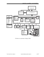
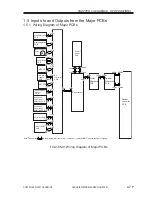
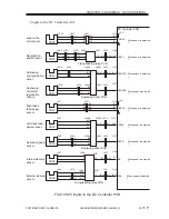
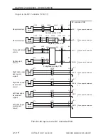
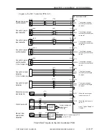
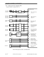
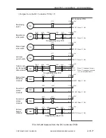
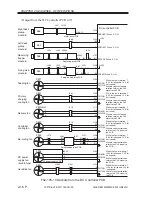
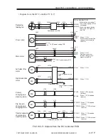
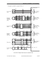
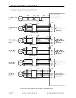
1.5 Inputs to and Outputs from the Major PCBs
1.5.1 Wiring Diagram of Major PCBs
Controller unit
DC
controller
PCB
BD PCB
Motor driver
PCB
Potential control
PCB
Environment
sensor
PCB
Cassette 3
paper level
detection PCB
Cassette 4
paper level
detection PCB
Duplexing driver
PCB
HVT PCB
J103
Laser scanner
motor
J116
Laser driver
PCB
J102
J113
DC power
supply
PCB
J101
J113
J113
AC driver PCB
J102
J107
J1015
J122
J6801
J1018
J6505
J1012
J120
J104
J105
J2701
J2101
J2108
Control
panel
PCB
M15
J810
J2052
J806
J8492
J4502
J4003
J2511
J2302
J3
Note: The symbol in the diagram indicates major connections, and does NOT indicate the flow of signals.
J121
J2501
J117
J2502
J1061
Reader
controller
PCB
Reader
Differential
PCB
J5008
J5502
J9201
J5503
Printer
Differential
PCB
J9203
J5004
J5501
F02-105-01 Wiring Diagram of Major PCBs

