COPYRIGHT © 2001 CANON INC.
2000 2000 2000 2000
CANON iR5000i/iR6000i REV.0 JUNE 2001
CHAPTER 1 GENERAL DESCRIPTION
1-28 S
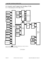
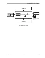
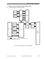
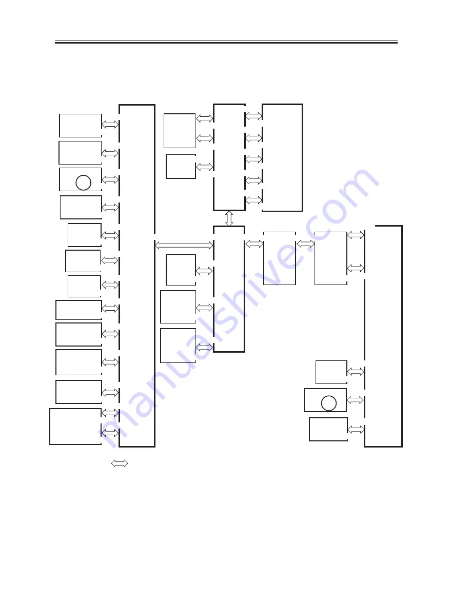
5.3 Inputs to and Outputs from the Major PCBs
5.3.1 Wiring Diagram of the Major PCBs
F01-503-01
Controller
assembly
DC
controller
PCB
Hard
disk
BD PCB
CCD/AP
PCB
Motor driver PCB
Potential
control PCB
Environment
sensor PCB
Cassette 3
paper level
detection PCB
Cassette 4
paper level
detection PCB
Duplexing
driver PCB
Scanner motor
Inverter PCB
HVT PCB
Reader
controller
PCB
J103
Control
card IV
(accessory)
Copy data
controller
(accessory)
J1060
J1022
J5011
Laser scanner
motor
J5101
J116
J5007
Laser driver
PCB
J121
J102
J113
DC power
supply PCB
J101
J113
J113
AC driver PCB
J102
J107
J1015
J122
J1017
J6801
J1018
J120
J5003
J104
J105
J2701
J6002
J2101
J2108
J1551
J1532
J1530
Numeric
keypad PCB
LCD panel
(LCD)
Inverter
PCB
Control
panel
CPU
PCB
J6504
J6509
J6604
Reader
Differential
PCB
J5008
J5502
J9201
J1061
J5503
Printer
Differential
PCB
J9203
J5004
J5501
J6506
J6507
J6503
M3
M15
J6502
J6601
J6602
J6501
J6603
J6508
J6605
J956
J810
J2052
J806
J8492
J4502
J4003
J2501
J2511
J2302
J3
Note: The symbol in the diagram indicates major wiring connections,
and does not indicate the flow of signals.

