POWER SUPPLY REVISIONS
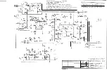
Beginning with serial number PS1006, a number of changes were made to improve overall performance. The
most significant change being the snubber network (C27
&
R62). This change increases the flyback energy
absorbing capability by a factor of five and consequently the overall reliability under adverse conditions is
improved. Refer to appendix A for these changes and updating procedures.
230 VOLT (EUROPEAN VERSION) POWER SUPPLY
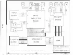
In mid year 1989, a 230 volt version of the PM-2.0t was introduced. Refer to the European version schematic
and Appendix B for the circuit changes. All test procedures for the 120 volt PM-2.0t apply to this unit. Due to
the fact that the switching transistors 06
&
07 have half the current rating of the domestic PM-2.0t, it is not
possible to make a voltage change between these two versions.
If
voltage conversion is absolutely necessary, it
can be accomplished only by changing the entire power supply module.
·
PM 2.0t
AMPLIFIER
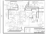
The power amplifier section of the 2.0t is very similar to the PM 1.5 series. The primary differences in the
PM2.0t are input muting, the addition of a fourth power supply rail, the power supply shut down circuitry and
parallel mono operation. This section will deal only with these areas.
Because the power supply has very limited output capability during the start up phase, the signal input to the
amplifier must be muted momentarily to allow the supply to complete it's start cycle and toggle into the high
power mode. This is accomplished with the muting FETs 0134/0334 and the drive circuit of 02.
When the amplifier is turned on, the gate to source voltage· on the muting FETs is zero which puts the FETs in a
low resistance on state. Since they form a voltage divider with R 101/R301, the signal level to the input of Ul is
attenuated� 35dB.
As the power supply comes up to full power operation, the emitter of 02 is "hard" biased to -12V. With C7
across the base-emitter junction, this transistor remains in the off state momentarily which allows the muting
FETs to stay on. As C7 discharges through R5
&
R6, transistor 02 turns on causing the collector voltage to
swing negative which turns the muting FETs off. If a fault condition shuts the power supply down or the
amplifier is turned off, diode D3 provides a rapid discharge path for C7 and resets the mute FETs to their on
state.
The following fa ult conditions will cause the power supply to shut down.
a) A short circuit at the amplifier output:
b) DC off set voltage at the output terminals:
c) Temperatures in excess of 100° C at the output transistors:
d) Excessive out of band high frequency output:
Under short circuit conditions, 01 on the Amplifier circuit board is turned on which activates 07 on the power
supply Secondary circuit board. With 07 on, a conduction path for the LED section of U3 on the Primary
circuit board is completed causing the power supply to shut down and recycle to the start sequence.
page4


