— 33 —
2
SRAM MEMORY CHECK
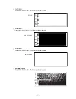
Press 1 button, the following display appears.
ROM SUM
(CS8)= XXXX
(CS7)= XXXX
SRAM CHECK
(128K)= OK
In case of abnormal S-RAM, NG display appears.
3
CHECK SUM
Press ESC, then 2 button. The following display appears.
ROM shown to this display indicates LSI301.
4
BUS CHECK
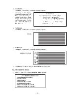
Press ESC, then 3 button. The following display appears.
SRAM CHECK
(128K)=
OK
ROM SUM
(CS8)= XXXX
(CS7)= XXXX
FLASH CHECK
(CS5)=
1M
XXX5
(CS4)=
1M
XXXXXXXX
XXX4
BANKXX
" (CS5)= 1M" indicates that the flash ROM of memory capacity 1M byte is mounted on Main PC
board as LSI304. If this ROM is not mounted, "NC" is displayed instead of "1M".
" (CS4)= 1M" indicates that the flash ROM of memory capacity 1M byte is mounted on Main PC
board as LSI306. "NC" is displayed in stead of "1M" because this LSI306 is not mounted with
BN-10. “XXX44” is not displayed with BN-10 also.
"XXX5(4)"- If "OKF5(4)" is displayed, the flash ROM of LSI304(LSI306) is formatted and have
no memories. If "NGF5(4)" is displayed, the flash ROM of LSI304(LSI306) is not formatted and
have memories.
If "OKB5(4)" is displayed, the wiring interior the flash ROM of LSI304(LSI306) is normal and
steady. If "NGB5(4)" is displayed, the wiring interior the flash ROM of LSI304(LSI306) is abnor-
mal and unsteady.
5
SRAM WRITE CHECK
Press ESC, then 4 button. The following display appears.
SRAM WRITE
END
Summary of Contents for BN-10
Page 1: ...R BN 10 ZX 456 BN 20 ZX 457 NOV 1997 without price BN 20 ...
Page 49: ... 49 Main block PCB ASSY A140806 2 5 FM3416 Gate array ...
Page 51: ... 51 Main block PCB ASSY A140806 4 5 LINE DRIVER RECEIVER ...
Page 52: ... 52 Main block PCB ASSY A140806 5 5 AC Adapter Batteries ...
Page 55: ... 55 Display block LCD ASSY A140809 A140814 2 3 LCD common terminal driver ...
Page 56: ... 56 Display block LCD PCB ASSY A140809 A140814 3 3 LCD segment terminal driver ...
Page 57: ... 57 Cradle A140805 BN 10 20 PCB Z456 1 shielded ...


