background image

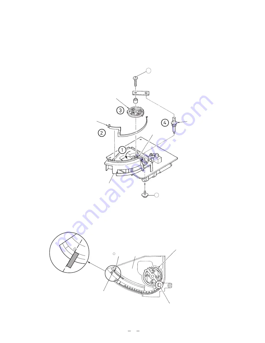
REASSEMBLY OF TUNING POINTER

1. Turn the varicon unclockwise stop position.
2. Set the pointer 

;

 mark position. (refer figure 6)

3. Set the varicon gear of figure 6 position.
4. Insert the tuner gear

Figure 6

3

Varicon Gear

Tuner Gear

Pointer

    Mark

Tuner Chassis

K

Figure 5

Varicon Gear

Pointer

Varicon

Tuner Gear

L

Tuner Chassis

Summary of Contents for CD-311S

Page 1: ... without price CD 311S CD RADIO CASSETTE PLAYER INDEX Model C Europe Model E Other Countries ...

Page 2: ...s 20 Tuner PCB Top View 20 CD AMP Door SW PCB Top View 21 VR PCB Top View 22 PS PCD Top View 23 Tape PCB Top View 24 LCD PCB Top View 25 Wiring Diagram 26 IC Lead Identification and Internal Diagrams 27 Schematic Diagrams 33 CD Mechanism 33 Tuner 34 AMP PS 35 Tape 36 CD 37 Parts List 38 Exploded Views 45 Cabinet 45 Cassette Mechanism 46 Case Unit 47 Top Case Unit 48 CD Mechanism 49 CONTENTS ...

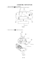
Page 3: ...e the battery cover and batteries 2 Remove six screws A holding case B ass y case B unit PS unit Figure 1 3 Remove four screws B holding the case ass y Case B Ass y Battery Cover CD Door Case Angle Top Case Ass y Case Ass y Figure 2 1 ...

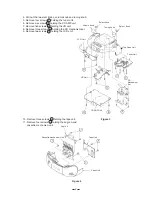
Page 4: ...r screws C holding the tuner unit 6 Remove six screws D holding the CD AMP unit 7 Remove five screws E holding the VR unit 8 Remove three screws F holding the CD mechanism set 9 Remove two screws G holding the LCD unit 10 Remove three screws H holding the tape unit 11 Remove four screws J holding the angle A and cassette mechanism unit Angle A Tape Unit Case Unit Cassette mechanism Unit Figure 4 2...

Page 5: ...e stop position 2 Set the pointer mark position refer figure 6 3 Set the varicon gear of figure 6 position 4 Insert the tuner gear Figure 6 3 Varicon Gear Tuner Gear Pointer Mark Tuner Chassis K Figure 5 Varicon Gear Pointer Varicon Tuner Gear L Tuner Chassis ...

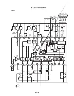
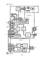
Page 6: ...IX AM RF In FM RF Out VCC 1 FM OSC AM OSC DET Out MPX In LPF1 LPF2 VCO GND VCC R ch L ch FM RF In GND1 FM MIX AM MIX AGC VCC 2 AM IF In FM IF In GND2 QUAD 3 1 2 4 To Amplifier Block 22 21 20 19 18 17 16 15 14 13 24 23 D3 Bar Antenna L1 L5 L4 L3 SW1 BAND SW AM FM Stereo FM MONO Rod Antenna L8 CF1 CF2 L9 FM Signal AM Signal L7 1 2 3 4 5 7 6 8 9 10 11 12 4 ...

Page 7: ...9V DC 9V GND BEAT SW101 REC PLAY IC101 PRE AMP L101 OSC TAPE BLOCK SW501 Beat Q620 Q720 Q623 Q723 AF MUTE IC581 PW AMP L ch R ch TU 9V GND CD 9V TU 9V Tape 9V DC 9V CD 9V TU 9V Tape 9V DC 9V AMP BLOCK VR201 Volume SW202 SW201 Function PS BLOCK To CD Block To Tuner Block AC BATT Speaker Headphone R P Head Audio Signal Recording Signal 5 ...

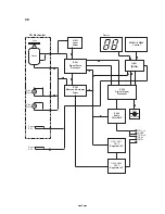
Page 8: ...cessor Q501 Laser Driver IC503 Motor and Actuator Driver IC502 Digital Signal Processor IC801 µ µ µ µ µ COM SW801 SW806 Control Display IC504 Audio Filter AMP X501 16 9 MHz CD L ch A GND CD R ch CD 9V GND Q501 Q511 D510 Regulator 5V Q504 Q505 D504 Regulator 8V Pset SW Door SW 6 ...

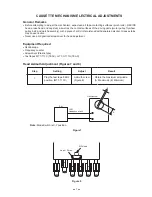
Page 9: ...e of soft cloth moistened with denatured alcohol Grease stains may cause trouble Never use a magnetized screwdriver for head adjustment Equipment Required Oscilloscope Frequency counter Screwdriver Plastic type Test tapes MTT 113C TEAC or TCC 111N TEAC Head Azimuth Adjustment Figures 7 and 8 Step Setting Adjust Result 1 Play the test tape 8 KHz position MTT 113C Azimuth screw Figure 8 Obtain the m...

Page 10: ...ures 9 and 10 Step Setting Adjust Result 1 Playthe test tape MTT 111N Motor screw Figure 10 Frequency counter reading should be 3000 Hz 2910 3090 Figure 10 Furequency Counter Figure 9 3000 Set J501 Headphone Jack 8 Motor screw ...

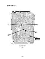
Page 11: ...ures 11 and 13 CD ADJUSTMENTS A B 0V Vref A B Step Connect Setting Adjust Result Play the test disc 1 See Figure 11 VR501 Set the PAUSE mode 2 Syncroscope CD PCB GND R572 TSO R571 Vref Figure 11 RF Adjustment Figures 12 and 13 Step Connect Setting Adjust Result Syncroscope CD PCB Adjust VR502 for the amplitude of the waveform at maximum VR502 Measuring on syncroscope Play the test disc See Figure ...

Page 12: ...10 CD Adjustment Points VR502 EF Balance RF VR501 TSO R572 RFO R570 Vref R571 Figure 13 CD PCB Top View ...

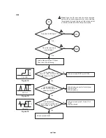
Page 13: ...OTING Is 00 display on LCD 1 2 Is the audio signal present at the output terminals 3 Press or key Can a selected of music be searched smoothly 4 OK No Yes No No Yes Yes Yes Load a disc and close CD door No Press key Is total track numbers displayed about 5 seconds 11 ...

Page 14: ... Check X501 Check circuit around X501 and IC502 Does 1 4 MHz clock pulse appear at IC801 pin 30 No Yes Check circuit around IC502 pin 72 Check and circuit around IC801 Check LCD Check wire connector 1 At power on 00 is not displayed 2 is not displayed total track numbers 2 How long times it takes until is displayed after CD door has closed A B About 5 sec About 16 sec 12 ...

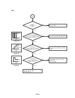
Page 15: ...CD door Then check the following Is the waveform at R570 RFO like that shown in Fig 15 Check around IC501 and IC502 Is the waveform at pin 21 SEL of IC501 like that shown in Fig 14 Check wire connector from pickup Check IC501 Check pickup Is the waveform at pin 10 FEO of IC501 like that shown in Fig 16 Check around pins 8 9 and 10 of IC501 Check VR502 Check around IC501 No No No No No Yes Yes Yes ...

Page 16: ...01 Is waveform at pin 42 SEL of IC502 like that shwn in Fig 18 Check around IC501 and IC502 SEL Is waveform at base of Q501 like that shown in Fig 19 Check around pin 45 of IC501 and Q501 Check IC501 Check 16P flat cable Check pickup No No No No Yes Yes Yes Yes Figure 17 Figure 18 Figure 19 5V 0V 5V 0V 0V 2 5V 3V A1 GND GND GND 14 ...

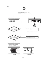
Page 17: ...503 like that shown in Fig 20 Check 16P flat cable Check pickup Is waveforn at pin 16 FSO of IC501like that shown in Fig 21 Is waveform at pin 17 COSC of IC501 like that shown in Fig 22 Check around IC503 Check around IC502 Check around IC501 No No No Yes Yes No Yes Yes 1V VREF COSC 4V Figure 20 Figure 22 VREF FSO Figure 21 1V 15 ...

Page 18: ...onnector CN543 and wire Check disc motor Is waveform at pin 40 DMPC of IC502 llike that shown in Fig 24 Is waveform at pin 24 DMEO fo IC501 like that shown in Fig 24 Check around IC501 and IC502 Check around IC501 and IC502 Yes Yes Yes Yes No No No No Check around IC501 and IC503 5V Figure 23 4V Figure 24 B 16 ...

Page 19: ...in 53 RFI of IC502 like that shown in Fig 25 B2 Is waveform at pin 60 PDO of IC502 like that shown in Fig 26 Check around pin 53 of IC502 Readjust VR502 Check around PLL of IC502 Check digital signal of IC502 and IC801 Check IC502 and IC801 No No Yes Yes Figure 25 Figure 26 B1 1 0 1 4V 4V 17 ...

Page 20: ... 28 Check 16P flat cable Readjust VR501 Check IC501 Check around TE Amp lines Check IC501 Check around TSO lines Check IC503 Check pickup 3 Check around IC502 pins 2 6 and IC504 Check D601 and D701 Check around IC601 No No No No Yes Yes Yes Yes Figure 27 Figure 28 B2 0 6V 1 5V 3V Does audio signal appear at IC504 pins 1 and 7 3 No present at output terminals audio signal 18 ...

Page 21: ...ector CN502 Check pickup Press the or key Is waveform at pin 36 FMFB of IC502 like that shown in Fig 31 Check around IC503 Check sled motor Is waveform at pin 33 TKIC of IC502 like that shown in Fig 32 Check around IC501 Check around pins 36 and 33 of IC502 Yes Yes Yes Yes No No No No Figure 29 Figure 30 Figure 31 Figure 32 Vref Vref 19 VREF TSO VREF FMFB VREF TKIC VREF VREF TSO A B A B A B 0 6V ...

Page 22: ...PCB VIEWS 20 Tuner PCB Top View ...

Page 23: ...21 CD AMP PCB Top View Door Switch PCB Top View ...

Page 24: ...22 VR PCB Top View ...

Page 25: ...23 PS PCB Top View C401 FUSE 2A 125V F400 AC 1 AC 2 CN400 BATT 2 BATT 1 AC9V GND DC9V C400 D401 D403 D402 D404 C402 C403 C404 JP400 JP401 PS PCB C2451 505 0 91 ...

Page 26: ...24 Tape PCB Top View ...

Page 27: ...25 LCD PCB Top View ...

Page 28: ... 1 9 1 6 1 1 2 3 1 2 1 2 Red Red White Red Red Shield Shield Shield Shield White White White 1 6 CN548 1 1 4 8 CN540 CN551 1 1 10 8 LCD PCB CD AMP PCB DOOR SW PCB 1 4 1 2 1 2 1 2 1 8 1 9 CN547 CN546 CN539 1 16 CN543 CN544 1 10 1 2 CN542 1 4 1 4 2 1 1 16 AC Socket Pickup Preset Switch Disc Motor Sled Motor Speaker L ch Speaker R ch 4 CD MECHANISM 1 2 Red 1 2 White Black To AC Socket SW10 To PS PCB ...

Page 29: ...n ALC R In NF PRE REC REC 1 12 24 13 FM AF AM AF FM IF AM IF FM RF 22 21 20 19 18 17 16 15 14 13 AM OSC FM OSC PRE VCO Decode SW HYS F F TUN LED ST LED FM DET AM FM SW Level DET AM DET AGC AM MIX FM MIX 24 23 1 2 3 4 5 7 6 8 9 10 11 12 AM RF In FM RF Out VCC 1 FM OSC AM OSC DET Out MPX In LPF1 LPF2 VCO L ch Out R ch Out FM RF In GND1 FM MIX AM MIX AGC VCC 2 AM IF In FM IF In GND2 TUN LED ST LED QU...

Page 30: ... 20k 20k 20k 20k 10k 10k TE ADD 25k 20µA 20k 10k 10k 68P TS 39P TP 7k 17 5k 24k 12k 100k TS1 47k 47k TS2 47k LD 20k 180k FMS DM 5P 68k 68k 1 35V 16k 10k BGR 2 8k 100µA MD 680 1k 1 27k 13k 33P 15k 15k 33P FE 20k 49k 22k 70k 150k 47k FS 30k 100k FSOSC 1 5k BOTTOM RFO RFI VRO 2VRO RFRP SBAD DFIN FEP FEN FEO FEI FHLD FEL1 FEL2 FSN FSO COSC OSCI GND VCC SEL DMEP DMEN DMEO RFT RFN MDI LDO FPI FNI TNO TN...

Page 31: ...onverter GNDA RO RO VDA LO LO GNDA TEST3 TEST4 TEST5 SBOK VDDD GNDD SUS0 BUS1 BUS2 BUS3 CCE BUCK 4MCK RST SUBSYC SUBD CLCK Correction Sydtem Timing Generator Internal Status SYNC Separation Circuit EFM Demodurarion Circuit DMPC DMFC DMON TEST FMFB TEST1 FMON TKIC TGUH1 TGUH2 TGUL TEL1 TEL2 DFCT GNDD VDDD 2VREF SEL FCSI FKIC FEL2 FEL1 FEI TESH TEOF SBAD RFRP VREF RF1 GNDA DTSC2 MONIT DTSC1 VDDA PDC...

Page 32: ...7 26 25 24 23 22 21 20 19 18 17 16 15 1 2 3 4 5 6 7 8 9 10 11 12 13 14 Level shift Level shift Level shift Level shift MUTE 13 3K VIN4 VIN4 VIN3 VIN3 OP Out OP In OP In 10K 10K 13 3K 13 3K 13 3K 10K 10K GND NC VCC VO3 VO3 VO4 VO4 VCC BIAS In VIN1 VIN1 VIN2 VIN2 GND GND MUTE VCC VO2 VO2 VO1 VO1 28 15 1 14 ...

Page 33: ...1 TA8227P 12 1 3 4 6 5 8 2 7 11 10 Bias Circuit Thermal Shut Down Protection Circuit 9 Vcc1 Vcc2 B S 1 Out 1 Power GND 30 kΩ 45Ω In 1 NF 1 Ripple In 2 NF 2 30 kΩ 45Ω Pre GND F In OUt 2 B S 2 Ch 1 Ch 2 1 6 12 7 ...

Page 34: ...32 IC801 TMP47C422F FR11 ...

Page 35: ...33 CD Mchanism Disc M M P set Switch Sled Motor Disc Motor 1 2 3 4 6 7 8 9 10 11 12 13 5 14 15 16 SCHEMATIC DIAGRAMS ...

Page 36: ...R 8 S V R 1 1 0 K B 1 N 4 1 4 8 1 N 4 1 4 8 1 5 K 1 5 K R 1 0 R 9 C1 9 1 0 0 1 6 C2 0 0 0 2 2 R D5 1 A D3 S W1 BA N D S W 4 3 2 1 T A 8 1 6 7 N A MR F MR V C1 F O S A O S DET MP X P F 1 P F 2 V CO L O R O Q U D S L T L G D2 F I F A T F V CC A G C A MM F MM G D1 F MI 2 4 2 3 2 2 2 1 2 0 1 9 1 8 1 7 1 6 1 5 1 4 1 3 1 2 1 1 1 0 9 8 7 6 5 4 3 2 1 J P M P J 4 R 4 1 0 0 1 N 4 1 4 8 D2 C9 3 3 0 0 P F 0 0...

Page 37: ... F0 047 4 3 SP1B RIGHT 2 1 SP1A LEFT L R SPEAKER 4 3 2 1 CW542 2451 542 2 5pitch 1 2 3 4 CN542 4pin 2 5pitch C590 470u 16V R591 47 1 4W C588 22u 16V R590 100K C732 22u 16V C580 220u 16V R722 1K R721 560K Q720 2SC1815 C723 0 47u 50V C720 1u 50V R ch TU 9V GND TO TUNER TAPE TAPE 9V L ch R ch 8 7 6 5 4 3 2 1 CN540 8pin 2 5pitch 1 2 3 4 5 6 7 8 CW540 2446 540 2 5pitch R720 22K R723 1K C722 1u 50V C721...

Page 38: ...u 50V C112 0 0022u M R124 1K R114 220K C116 1u 50V C114 22u 16V R110 68K C118 1u 50V 9 10 11 12 13 14 C136 47p CH C119 0 0047u B C121 220p B C117 10p CH R130 4 7K C133 10u 16V R127 100K R128 47K R129 10K 15 16 R123 100 1 4w L ch TAPE 9V R ch DC 9V REC L ch GND 1 2 3 4 5 6 7 8 JP F PJ 8 REC R ch BEAT C134 1u 50V D104 1N4148 R115 20K R111 82 C115 0 01u M C131 0 01u M C120 0 0027u B R113 10K C D TL R...

Page 39: ... P 3 3 T S 1 P 3 4 T S O 3 5 T E L 1 3 6 T E L 2 3 7 T S N 3 8 TPO 39 TPI 40 TNI 41 TNO 42 FNI 43 FPI 44 LDO 45 MDI 46 RFN 47 RFT 48 C547 0 1u M C516 10u 16V VR PD LD C B D A E F 5V VREF R502 56K R503 56K R504 56K R505 56K R507 68K R506 68K R501 91 R508 130K VR501 100K R509 180K D501 1N4148 C501 1u 50V R515 56K 1 2 3 4 5 6 7 8 9 10 11 12 13 14 15 16 CN539 16pin 16 15 14 13 12 11 10 9 8 7 6 5 4 3 2...

Page 40: ... specifications are subject to change without pointer notice 2 As for spare parts order and supply refer to the GUIDEBOOK for Spare parts Supply published separately 3 The numbers in item column correspond to the same numbers in drawing 38 ...

Page 41: ...8 060 0 00 1 C VARIABLE RESISTORS N VR 501 1915 7392 POTENTIOMETER TRIMMER 100K C0031 779 1 04 1 C N VR 502 1915 7393 POTENTIOMETER TRIMMER 5K C0031 779 5 02 1 C OSCILLATOR X 501 1910 0333 RESONER CERAMIC FCR16 93M2G 0038 988 0 00 1 C TAPE UNIT IC N IC 101 1915 7363 IC TA7668BP 0911 201 8 00 1 A COIL N L 101 1915 7364 OSC TRANS 10 MT216 1188 C0015 098 0 00 1 C TRANSISTOR Q 101 102 1909 3379 TRANSI...

Page 42: ...B MODE C2446 867 0 01 1 C N 8 1915 7466 KNOB BBS C2446 869 0 01 1 C N 9 1915 7470 COVER BATTERY C2451 808 0 03 1 C N 10 1915 7473 KNOB TUNING C2451 873 0 03 1 C N 11 1915 7475 KNOB VOLUME C2451 874 0 03 1 C N 12 1915 7477 KNOB SELECT C2451 875 0 03 2 C N 13 1915 7410 UNIT TAPE MECHA SET 2446 100 0 00 1 B TK20FX V644 001 N 13 1 1915 7398 BUTTON REC C2446 860 0 01 1 C N 13 2 1915 7400 BUTTON PLAY C2...

Page 43: ... C Model C CD MECHANICAL PARTS 16 1 1015 0903 LASER PICK UP SPU3201 0020 016 0 0001 1 B N 16 2 1915 7452 MOTOR MCR3B 0022 105 0 0013 1 C N 16 3 1915 7453 MOTOR BCH3B 0022 106 0 0013 1 C N 16 4 1915 7454 CENTER TABLE 2516 271 1 00 1 X 16 5 1909 8291 SPRING COM 2595 400 1 00 1 X N 16 6 1915 7455 GEAR MOTOR 2596 260 0 00 1 X 16 7 6925 0850 GEAR A 2596 261 0 00 1 X N 16 8 1915 7456 SUB RACK 2596 263 1...

Page 44: ... C537 Ceramic 50V 0 047 µF 80 20 1 C538 Ceramic 50V 0 047 µF 80 20 1 C539 Electrolytic 10V 47 µF 20 1 Item Specification Q ty C1 Ceramic 50V 22 PF 5 1 C2 Ceramic 50V 25 PF 5 1 C3 Ceramic 50V 5 PF 0 25 PF 1 C4 Ceramic 50V 22 PF 5 1 C5 Ceramic 50V 8 PF 0 5 PF 1 C6 Ceramic 50V 0 022 µF 10 1 C7 Ceramic 50V 0 022 µF 10 1 C8 Ceramic 50V 0 022 µF 10 1 C9 Ceramic 50V 15 PF 5 1 C10 Ceramic 50V 33 PF 5 1 C1...

Page 45: ...lytic 16V 220 µF 20 1 C581 Electrolytic 16V 100 µF 20 1 C582 Electrolytic 10V 220 µF 20 1 C583 Ceramic 50V 0 047 µF 80 20 1 C588 Electrolytic 16V 22 µF 20 1 C589 Electrolytic 10V 47 µF 20 1 C590 Electrolytic 16V 470 µF 20 1 C592 Electrolytic 16V 1000 µF 20 1 C594 Ceramic 50V 1000 PF 10 1 C595 Ceramic 50V 0 047 µF 80 20 1 C601 Ceramic 50V 330 PF 10 1 C602 Ceramic 50V 1500 PF 10 1 C603 Ceramic 50V 1...

Page 46: ...1 R825 47KΩ 10 R834 R840 4 7KΩ 1 R841 10KΩ 1 R842 19KΩ 1 R843 560KΩ 1 R850 1KΩ 1 4W 1 Item Specification Q ty R502 56KΩ 4 R505 R506 68KΩ 1 R507 68KΩ 1 R508 130KΩ 1 R509 180KΩ 1 R510 22Ω 1 4W 1 R511 51KΩ 1 R512 39KΩ 1 R513 22KΩ 1 R514 680KΩ 1 R515 56KΩ 1 R516 1 5KΩ 1 R517 68KΩ 1 R518 2 7KΩ 1 R519 680KΩ 1 R520 470KΩ 1 R521 51KΩ 1 R522 39KΩ 1 R523 820Ω 1 R526 27KΩ 1 R527 8 2KΩ 1 R529 1 5MΩ 1 R530 1KΩ...

Page 47: ...EXPLODED VIEWS 45 12 11 7 15 6 4 8 3 1 1 2 14 1 2 2 12 10 18 J301 T001 9 17 19 5 L001 2 Cabinet S 10 ...

Page 48: ...Cassette Mechanism 46 13 1 13 2 13 3 13 4 13 5 13 6 13 ...

Page 49: ...47 Case Unit 14 7 14 4 14 2 14 6 14 3 14 1 15 8 14 8 14 7 14 5 ...

Page 50: ...48 Top Case Unit 15 2 15 4 15 3 15 5 16 15 7 15 6 15 1 14 8 15 8 ...

Page 51: ...49 CD Mechanism 16 4 16 10 16 5 16 9 16 16 16 2 16 6 16 3 16 8 16 11 16 1 16 7 16 14 16 13 16 15 16 12 ...

Page 52: ...AF0400181A CASIOTECHNO CO LTD Overseas Service Division 8 11 10 Nishi Shinjuku Shinjuku ku Tokyo 160 0023 Japan ...

Reviews: