— 19 —
5-5. Individual function test
1) Series test
This test will perform the following tests in series.
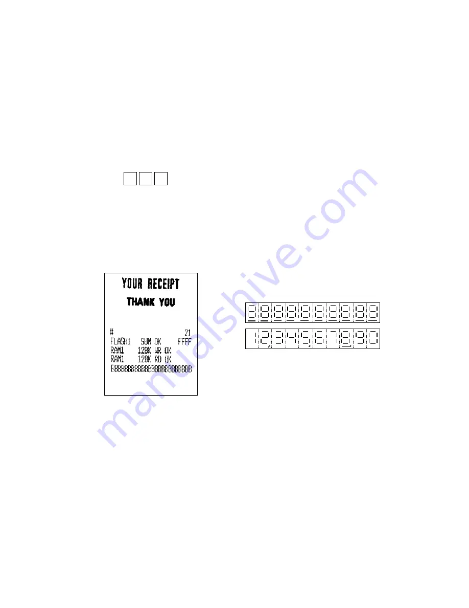
1. Display test (All dot and segment trun on.)
2. RAM read after write test (one time)
3. Print test (one time)
4. Time display test
5. Drawer open test
6. Receipt issue test
7. Display test (1234567890 display)
Operation :
X
1
#2 Key
Function
X: 0= Automatic RAM capacity detection
1= RAM1 (128K) test only
NOTE : CE-6800 has the only RAM1 (128 K bytes).
[PRINT]
[DISPLAY]
NOTE : In case of error, the following error message will be printed.
RAM1 128K WR ERR!!
00 000000 ----------- When the write error is happened.
Error Bank and Address
RAM1 128K RD ERR!!
00 000000 ----------- When the verified data error is happened.
FLASH SUM ERR!!
1234 ----------- Check sum of Flash1 is not "FFFF".
Caliculated check sum
Summary of Contents for CE-6800
Page 5: ...3 2 BLOCK DIAGRAM 2 1 PCB CONNECTION...
Page 31: ...29 5 HIN211CA T 7 LC7932M TE R 6 HY628100ALLG 70...
Page 33: ...31 9 LM2576HVT 5 0LB03 10 MTA001M F4101...
Page 35: ...33 15 SN74LV00APWR 16 SN74LV02APWR 14 SN74HC27PWR 17 SN74LV08APWR...
Page 36: ...34 18 SN74LV138APWR 19 SN74LV139APWR...
Page 37: ...35 20 SN74LV165APWR...
Page 38: ...36 21 SN74LV165APWR 22 SN74LV174APWR...
Page 39: ...37 23 SN74LV32APWR 24 SN74LV74APWR...
Page 40: ...38 7 PCB LAYOUT MAIN PCB Front side...
Page 41: ...39 MAIN PCB Back side...
Page 43: ...41 CASIO COMPUTER CO LTD CE 6800 EX 475P Model Name SYSTEM BLOCK DIAGRAM Drawing No E140329P...
Page 44: ...42 42...
Page 45: ...43 RAM3 and RAM4 are option For CE6800 the Flash ROM2 is not used...
Page 46: ...44...
Page 47: ...45...
Page 48: ...46...
Page 49: ...47 DRW3 and DRW4 are not used...
Page 50: ...48...
Page 51: ...49...
Page 52: ...50...
Page 53: ...51...
Page 54: ...52...
Page 55: ...53 Voltage selector is not used for CE 6800...
Page 56: ...54...
Page 57: ...55...
Page 72: ...70 13 DRAWER DL 2771...


