background image

— 25 —

NOTE: When use the command ptrint and display, press #1 key (Cash AMT tender key) to display and

print the next line. To stop this test, press any key or set the mode switch to OFF position.

[PRINT]

[DISPLAY]

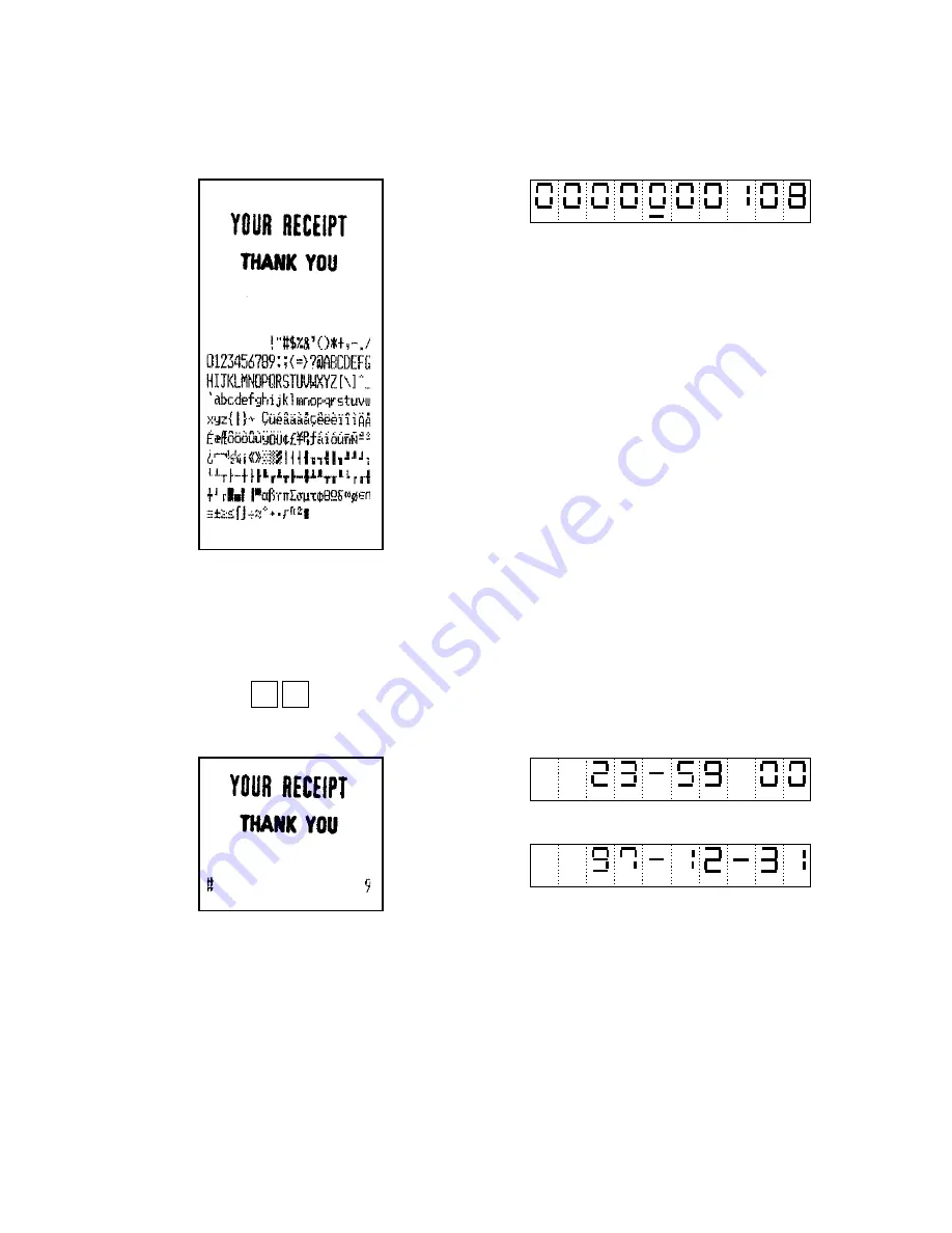
11) Time and date display test

The machine will display the time .
By  #2  Key, the display will change the date and time.

Opeartion :

9

#2 Key

[PRINT]

[DISPLAY]

Press #2 key to change the display.

Summary of Contents for CE-6800

Page 1: ...SERVICE MANUAL ELECTRONIC CASH REGISTER without price CE 6800 EX 475EP MAY 2001 Printer Model M U420B 031 INDEX...

Page 2: ...address circuit 12 4 6 Memory map 12 4 7 Printer drive circuit 13 4 8 RS232C port COM1 circuit 14 4 9 RS232C port COM2 and COM3 circuit 15 4 10 To mount optional circuit 16 5 DIAGNOSTIC OPERATION 17...

Page 3: ...ess Thickness 75 15 m 1 2 Environmental specifications Operating temperature 0 C 40 C Operating humidity 10 90 Storage temperature 25 C 65 C Storage humidity 10 95 Vibration strength 1 5 G The machine...

Page 4: ...to drive until 2 printers External printer UP 250 Connect to Com 1 2 or 3 It is possible to drive until 2 printers Scale Model 6710 Com 3 only NCI model Slip printer cable PRT CB 8C Connect Com 2 or...

Page 5: ...3 2 BLOCK DIAGRAM 2 1 PCB CONNECTION...

Page 6: ...COM3 Driver Driver Display driver and Key control circuit Main display Dot segment Customer display Keyboard ARCNET driver IN Line MAIN PCB E457 1 C RAM1 HY628100A LLG 70 128 K bytes RAM3 Option HM62...

Page 7: ...e upper case 3 Push the 3 dots marking point at the right side of lower case At the same time slide the upper case to the front side 4 Open upper cese from the left side Open the printer cover Remove...

Page 8: ...located as shown in the picture Battery Flash ROM 1 2 Mbytes Main PCB RAM 1 128 Kbytes RAM 4 Option RAM 3 Option COM 1 port CPU Buzzer Printer cable Display cable Power supply connector Reset Switch K...

Page 9: ...GND Signal GND The power switch SW1 is located at the right side of the lowercase After connected the power plug into AC outlet and turn on the SW1 the transformer T1 will genarate the about AC33V to...

Page 10: ...for the hard reset to cleare the system error Use this switch only when the FMAC or MAC are not possible to perform Reset switch The position of Reset switch From top of view From rear of view 4 3 CPU...

Page 11: ...ontroller In 23 AVDD VDD Power supply VDD 5V 24 AVREF0 AVREF0 Connected to VDD 5V 25 P10 AVREF Vp voltage check terminal In 26 P11 HDTH Head thermistor input In 27 P12 CROM IN Flash ROM cassette in si...

Page 12: ...ower supply GND 73 P60 A16 Address bus A16 Out 74 P61 A17 Address bus A17 Out 75 P62 A18 Address bus A18 Out 76 P63 A19 Address bus A19 Out 77 P64 RD Read signal Out 78 P65 WR Write signal Out 79 P66...

Page 13: ...A7 A6 A5 A4 A3 A2 A1 A0 L L H H X X X X X X X X X X X X X X X X 3 X X X X Therefore the RAM1 CE will active when the CPU adress is from 20000H to 3FFFFH with RAM enable signal H Flash ROM1 selection...

Page 14: ...X H X H X 11 H L L H H X X X H X H X 12 L H L H H X X X H X H X 13 H H L H H X X X H X H X 14 L L H H H X X X H X H X 15 H L H H H X X X H X H X 16 L H H H H X X X H X H X 17 H H H H H X X X H X H X L...

Page 15: ...0FFD0h External I O Mapping 16bytes 0FFE0h 20000h RAM1 128 K bytes 40000h Not used 80000h Bank area Flash 1 384 K bytes 16 M bit for A0000h Application 8 M bit program area 4 M bit 2 M bytes Bank0 Ba...

Page 16: ...14 4 8 RS232C port COM1 circuit The COM1 circuit is as follows The COM1 port pin location is as shown below 1 6 7 8 9 2 3 4 5 Signal CD RxD TxD DTR GND DSR RTS CTS CI 1 2 3 4 5 6 7 8 9 Pin...

Page 17: ...and COM3 are as follows TP48 The COM2 and COM3 port pin locations are as shown below COM2 COM3 COM2 port COM3 port 1 6 7 8 9 2 3 4 5 Signal NC RxD TxD DTR GND DSR RTS CTS NC 1 2 3 4 5 6 7 8 9 Pin Sign...

Page 18: ...it 1 Multi drawer kit Only Drawer 2 1 1 Prepare the following parts kit for multi drawer circuit The parts kits are supplied from sales division MDL 10 Multi drawer kit 1 2 Check whether the parts of...

Page 19: ...on of each test 1 Key code test When pressing a key the machine displays the following key code HARD KEY CODE TABLE Hard key code DISPLAY Note 014 button is work for 2 key 013 button is work for 1 key...

Page 20: ...ad down ON Head up Journal paper sensor Off Paper in ON Paper out Receipt paper sensor Off Paper in ON Paper out Mode switch status 0 No connetion 1 PGM 2 RF 3 REG1 4 REG2 5 X 6 Z 7 XZ2 8 OFF ROM cass...

Page 21: ...isplay test 1234567890 display Operation X 1 2 Key Function X 0 Automatic RAM capacity detection 1 RAM1 128K test only NOTE CE 6800 has the only RAM1 128 K bytes PRINT DISPLAY NOTE In case of error th...

Page 22: ...print 1 Continuously print n1 0 Display test pattern 1 All segment will light on PRINT DISPLAY Segment display Test pattern 3 Print test R J printer This test will check the R J printer To stop the co...

Page 23: ...be printed after this sample data Operation 9 0 0 2 Key PRINT DISPLAY 5 Drawer open check This test will check the drawer open function Operation d3 d2 d1 8 n 0 2 Key Function n 0 Open drawer without...

Page 24: ...op the test set the mode switch to OFF NOTE During the RAM test the Receipt switch LED is blinking PRINT DISPLAY 7 RAM read write check This test will check the read write check for RAM Operation n 4...

Page 25: ...op check continuously Ignore the CD CI signals Only COM1 port X 0 COM1 Test details 1 Check of the control shignals CTS DSR RTS DTR CD CI Low High level 2 Sending data 0A5h from Txd line and receiving...

Page 26: ...USA 02 Multilingual 01 France 03 Portuguese 02 Germany 04 Canadian French 03 England 05 Nordic 04 Denmark I 19 Euro Multilingual 05 Sweden 51 Czecho Poland 06 Italia 52 Hebrew 07 Spain 53 Greece 09 N...

Page 27: ...and print the next line To stop this test press any key or set the mode switch to OFF position PRINT DISPLAY 11 Time and date display test The machine will display the time By 2 Key the display will...

Page 28: ...COM1 COM1 Cable length Max 15m Opeartion z z b m 7 2 X 7 2 Key Function b Baud rate selection 0 19 200 bps 1 9 600 bps 2 4 800bps 3 2 400bps 4 38 400 bps m Test Mode selection 0 Self loop test 1 Recep...

Page 29: ...st block data wait time is 5 seconds The total resend request time is 5 time 3 During communication waiting time the display will show the brinking on the most left side digit of segment display When...

Page 30: ...7431PA 4 HD74LVC374ATELL BA10393 BA10393F 1 1ch 2 3 4 OUT1 IN1 IN1 VEE 8 7 6 5 VCC OUT2 IN2 IN2 2ch REF 2 500 V A K REF A TO 92MOD K 1 2 3 1 2 3 4 5 6 7 8 IN1 IN2 IN3 IN4 IN5 IN6 IN7 GND 16 15 14 13 1...

Page 31: ...29 5 HIN211CA T 7 LC7932M TE R 6 HY628100ALLG 70...

Page 32: ...decoders and sense amplifiers CE high deselects the device and reduces power consumption to standby levels CE INPUT WRITE ENABLE Controls writes to the CUI and array blocks Addresses and data are lat...

Page 33: ...31 9 LM2576HVT 5 0LB03 10 MTA001M F4101...

Page 34: ...HC157APWR 1 Nch open drain active low output 2 CMOS active low output S 808XX AX XX XXX T2 Tape spec IC direction Production short No Package No NP SC 82AB MP SOT 23 5 UP SOT 89 3 Y TO 92 Output N Nch...

Page 35: ...33 15 SN74LV00APWR 16 SN74LV02APWR 14 SN74HC27PWR 17 SN74LV08APWR...

Page 36: ...34 18 SN74LV138APWR 19 SN74LV139APWR...

Page 37: ...35 20 SN74LV165APWR...

Page 38: ...36 21 SN74LV165APWR 22 SN74LV174APWR...

Page 39: ...37 23 SN74LV32APWR 24 SN74LV74APWR...

Page 40: ...38 7 PCB LAYOUT MAIN PCB Front side...

Page 41: ...39 MAIN PCB Back side...

Page 42: ...2 MAIN PCB CIRCUIT 2 6 42 2 3 MAIN PCB CIRCUIT 3 6 43 2 4 MAIN PCB CIRCUIT 4 6 44 2 5 MAIN PCB CIRCUIT 5 6 45 2 6 MAIN PCB CIRCUIT 6 6 46 3 LED DISPLAY MAIN DISPLAY 47 3 1 MAIN PCB CIRCUIT 1 3 47 3 2...

Page 43: ...41 CASIO COMPUTER CO LTD CE 6800 EX 475P Model Name SYSTEM BLOCK DIAGRAM Drawing No E140329P...

Page 44: ...42 42...

Page 45: ...43 RAM3 and RAM4 are option For CE6800 the Flash ROM2 is not used...

Page 46: ...44...

Page 47: ...45...

Page 48: ...46...

Page 49: ...47 DRW3 and DRW4 are not used...

Page 50: ...48...

Page 51: ...49...

Page 52: ...50...

Page 53: ...51...

Page 54: ...52...

Page 55: ...53 Voltage selector is not used for CE 6800...

Page 56: ...54...

Page 57: ...55...

Page 58: ...without parts code 5 Remarks Q ty Quantity used per unit RANK A Essential B Stock recommended C Less recommended X No stock recommended 9 PARTS LIST PARTS LIST MODEL CE 6800 EX 475EP CONTENTS EXPLODE...

Page 59: ...E 6800 LED Numeric LED PCB Blank 0 00 1 2 3 4 5 6 7 8 9 D F A A F 11 5 4 3 55 10 7 6 8 9 39 38 33 34 32 28 30 29 37 13 14 12 18 15 16 17 20 25 21 47 22 27 23 19 2 52 85 86 51 48 46 49 56 82 31 50 56 2...

Page 60: ...58 Battery only For Drawer fix C D E C E B B 54 53 70 70 77 73 76 87 84 61 78 70 75 74 41 43 79 40 44 80 62 64 63 66 66 1 72 45 57 81 42 67 69 86 71 71 83 65 58 59 60 68...

Page 61: ...AA B D2 3 5 10 23901820 DIODE 1SS355TE 17 4 AA B D22 23153127 DIODE ZENER PTZTE 2522A 1 AB B D4 23153125 DIODE ZENER RD22UJN1 T1 1 AA B D6 9 11 16 23 23902058 DIODE 1SR154 400TE25 9 AB B FB12 3000809...

Page 62: ...T 1 X R2 RESISTOR CHIP RC1608 154 F T 1 X R23 RESISTOR CHIP RC1608 563 F T 1 X R24 44 RESISTOR CHIP RC1608 472 F T 2 X R26 RESISTOR CHIP RC1608 104 J T 1 X R27 RESISTOR CHIP MCR03EZHF3600 1 X R28 RESI...

Page 63: ...N 8 62481475 CABLE FFC JOINT DE445 E440657 4 1 AU C N 9 62481476 CABLE FFC JOINT EE445 E440657 5 1 AU C 10 62481785 CASE REAR DISPLAY E240511A 1 1 AH C N 11 10049340 PLATE REAR DISPLAY E240512A 8 1 AL...

Page 64: ...2482177 PLATE L E240527 17 1 X 62482178 PLATE L E240527 18 1 X 62481453 PLATE L E240527 8 1 X 62481454 PLATE L E240527 9 1 X 62481443 PLATE L E240527 10 1 X 62481444 PLATE L E240527 11 1 X 62481445 PL...

Page 65: ...7 Clerk switch circuit 24088399 LED GL3EG8 4 AA B 34121029 SW TACT SKHHAL 4 AA B 62481474 CABLE FFC JOINT E440657 3 1 AC C 62481473 CABLE FFC JOINT E440657 2 1 AC C 24088400 CONNECTOR HLW24R 2C7 1 AC...

Page 66: ...4X14 ZMC 3 3 X SCREW 4X35 ZMC 3 1 X SCREW 4X8 ZMC 3 1 X SCREW 4 1 X SCREW 3X4 ZMC 3 1 X SCREW 3X12 ZMC 3 2 X SCREW 3X5 ZMC 3 1 X 69B 62481472 SCREW E445 E440656 1 4 AB X TIE INSULOCK T 18S 1 X 10 Prin...

Page 67: ...904 903 902 905 119 125 125 130 907 501 134 137 102 101 108 126 127 122 117 116 118 906 510 123 121 142 135 131 RIBBON CASSET 133 132 130 138 139 145 140 128 129 120 124 115 110 508 514 513 512 510 1...

Page 68: ...539 539 533 549 548 549 548 538 531 532 532 532 529 531 528 527 535 541 540 545 544 542 526 537 525 704 708 709 709 117 716 710 703 714 711 706 701 702 116 723 716 719 715 723 723 706 723 723 724 724...

Page 69: ...028031 1 AH B 121 1906 0731 GEAR TRANSMISSION 1028009 1 AB B 122 1906 0802 GEAR DECELERATION 1028011 1 AC B 123 1906 0732 GEAR TRANSMISSION CARRIAGE 1028010 1 AD B 124 1906 0733 GEAR RIBBON DECELERATI...

Page 70: ...PAPER FEED TRIGGER F701251080 3 AB C 526 1906 0762 PLATEN ASSY 1028543 1 AS C 527 1906 0763 SHAFT PAPER FEED ASSY 1028544 1 CH A 528 9487 0513 SHAFT PAPER EXTENSION ASSY 1059877 1 BF C 529 1906 0804 S...

Page 71: ...EAR 2 1028084 1 AF X 716 1907 4057 RING RETAINING TYPE E 2 B150300411 3 AA C 717 1907 7216 SCREW M2X4 B010101311 2 AA X 718 1906 0793 PLATE CIRCUIT BOARD 1028096 1 AD C 719 1906 0794 CLAMP MINI 102919...

Page 72: ...70 13 DRAWER DL 2771...

Page 73: ...21 94870396 SCREW CCST M4X12 4 AA X 22 19064018 EARTH LEAF SPRING 33V 1103 1 AN X 23 19064008 SCREW CCST M3X6 1 AA X 24 94870574 SCREW CPDT M3X5 5 AA X 25 94870391 DRAWER 264C 2100 1 CM X 26 19077153...

Page 74: ...CASIO TECHNO CO LTD Overseas Service Division Nishi Shinjuku Kimuraya Bldg 1F 5 25 Nishi Shinjuku 7 Chome Shinjuku ku Tokyo 160 0023 Japan...

Reviews: