background image

— 12 —

3) Equipment connection/Procedure

Vop voltage setting

Output

Set

Voltmeter

TP1-TP2

Input
Connection

Input
Point

Input
Signal

Adjust

Output
Connection

Output
Point

Adjust for

VR501

Voltmeter

TP1-TP2

Adjust for 4.2 to 4.3 V read-

ing on voltmeter under the
temparature 20 to 25 

°

C.

Make fine adjustment accord-
ing to the following instruc-
tion.

1Watching the LCD at 32.52

°

 angle to the horizontal, adjust Vop

voltage so that unenergized segments are seen dimly.

2Watching the LCD at 62.23

°

 (upper limit) angle, check to see the

segments completely.

32.52

°

62.23

°

LCD

Eye

Eye

(upper limit)

Summary of Contents for CTK-631

Page 1: ...EN 108 KALIMBA 109 BAG PIPE 110 FIDDLE 111 SHANAI 112 TINKLE BELL 113 AGOGO 114 STEEL DRUM 115 WOOD BLOCK 116 TAIKO 117 MELODIC TOM 118 SYNTH DRUM 119 REVERSE CYMBAL 121 BREATH NOISE 122 SEASHORE 120 GT FRET NOISE 123 BIRD 124 TELEPHONE 125 HELICOPTER 127 GUNSHOT 128 159 167 199 160 168 126 APPLAUSE I N T RO SYNCHR O E N D I N G N O R M A L FILL IN VARIATI O N F I L L I N START STOP POWER TEMPO VO...

Page 2: ...CONTENTS Specifications 1 Block Diagram 3 Circuit Description 4 Adjustment 11 Major Waveforms 13 Printed Circuit Boards 14 Schematic Diagrams 17 Exploded View 24 Parts List 25 ...

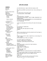
Page 3: ...mp envelope set attack rate release rate pitch envelope set pitch level touch sense pan Mixer function Channels 16 Parameters Program change number volume expression pan coarse tuning fine tuning on off solo MIDI 16 multi timbre receive GM Level 1 standard Other functions Pitch bend range 12 semitones upwards and downwards Transpose 25 steps 12 semitones to 12 semitones Tuning Variable A4 approxim...

Page 4: ... Vrms with 47k Ω load each channel L ch 3070 mV 20 with key A5 pressed in Bassoon tone R ch 2750 mV 20 Volume maximum Touch response maximum Reverb Hall Minimum operating voltage 6 3 V About General MIDI General MIDI standardizes MIDI data for all sound source types regardless of manufacturer General MIDI specifies such factors as tone numbering drum sounds and available MIDI channels for all soun...

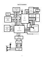
Page 5: ...rter IC1 UPD6379GR Filter Q308 Q311 Main Volume Power Amplifier IC301 TA8248K Keyboard MA0 MA19 Effect RAM 256K bit LSI5 TC55257DFL 70L EL MD0 MD7 Speakers Output MA0 MA14 MA0 MA1 LRCK SO BCK SINK LCD LCD Driver LSI501 SED1278F2A SEG1 SEG40 IN OUT Reset IC IC2 RN5VD40AA RESET COM1 COM16 DSP LSI2 HG51B277FB 1 MD0 MD15 CPU LSI1 GT913F T Buttons Assingnable Jack PB4 VDD Power Switch NMI FI10 P23 PA0 ...

Page 6: ...2 G3 2 G 3 2 A3 2 A 3 2 B3 2 FI3 C4 1 C 4 1 D4 1 D 4 1 E4 1 F4 1 F 4 1 G4 1 SI3 C4 2 C 4 2 D4 2 D 4 2 E4 2 F4 2 F 4 2 G4 2 FI4 G 4 1 A4 1 A 4 1 B4 1 C5 1 C 5 1 D5 1 D 5 1 SI4 G 4 2 A4 2 4 2 B4 2 C5 2 C 5 2 D5 2 D 5 2 FI5 E5 1 F5 1 F 5 1 G5 1 G 5 1 A5 1 A 5 1 B5 1 SI5 E5 2 F5 2 F 5 2 G5 2 G 5 2 A5 2 A 5 2 B5 2 FI6 C6 1 C 6 1 D6 1 D 6 1 E6 1 F6 1 F 6 1 G6 1 SI6 C6 2 C6 2 D6 2 D 6 2 E6 2 F6 2 F 6 2 G...

Page 7: ...rates five voltages as shown in the following table VDD voltage is always generated The others are controlled by APO signal from the CPU NOMENCLATURE OF KEYS RESET CIRCUIT When batteries are set or an AC adapter is connected the reset IC provides a low pulse to the CPU The CPU then initializes its internal circuit and clears the working storage RAM When the power switch is pressed the CPU receives...

Page 8: ...n AC adaptor detection terminal 5 V when the keyboard is powered by batteries and becomes 0 V to cancel the APO function when AC adaptor is connected 9 AN1 Not used Connected to ground 10 AGND In Ground 0 V source 11 BCK Out Bit clock output 12 SO Out Serial sound data output 13 LRCK Out Word clock output 14 GND In Ground 0 V source 15 16 XLT0 XLT1 In Out 20 MHz clock input output 17 VCC In 5 V so...

Page 9: ...IGNABLE Jack input 5 SO Out Serial sound data output for the DAC 6 WCKO Out Word clock output for the DAC 7 VDD3 In 5 V source 8 TEST Not used 9 RESB In Reset signal input 10 VSS2 In Ground 0 V source 11 12 XIN XOUT In Out 20 MHz clock input output 13 WCKI In Word clock input from the CPU 14 SI In Serial sound data input from the CPU 15 BCKI In Bit clock input from the CPU 16 SINC In 1 MHz synchro...

Page 10: ...AM 62 66 70 74 78 VSS2 In Ground source 63 67 71 75 79 VDD2 In 5 V source 64 65 68 69 PA0 PA5 Out Button scan signal output 72 73 76 77 PA6 7 Out Not used Pin No Terminal In Out Function 1 22 SEG1 SEG40 Out Segment signal output 63 80 23 VSS GND 0 V source 24 25 OSC1 OSC2 In Out Terminals for the built in clock pulse generator The external resistor connected determines the oscillation frequency 26...

Page 11: ...e Synch signal Data Word clock Bit clock Data Word clock Bit clock DSP LSI2 HG51B277FB DAC IC1 UPD6379GR CPU LSI1 GT913F T L OUT R OUT SI LRCK CLK SO WCKO SCK1 SO LRCK BCK SINC SI WCKI BCKI FILTER BLOCK Since the sound signals from the DAC are stepped waveforms the filter block is added to smooth the waveforms DAC IC1 UPD6379GR The DAC receives 16 bit serial data output from the DSP The data conta...

Page 12: ...bootstrap capacitor 3 OUT2 Out Channel 2 output 4 VCC In 9 V source 5 OUT1 Out Channel 1 output 6 B S 1 Terminal for a bootstrap capacitor 7 Power GND In Ground 0 V source 8 Stand by In Power control signal input 0 V Off 9 V On 9 DC Terminal for a decoupling capacitor 10 NF1 In Negative feedback input 11 IN1 In Channel 1 input 12 IN2 In Channel 2 input 13 NF2 In Negative feedback input 14 15 Pre G...

Page 13: ... 11 ADJUSTMENT DISPLAY PCB 1 Items to be adjusted 2 Adjustment and Test Point Locations TOP VIEW Item Measuring Instrument Vop voltage setting Voltmeter BOTTOM VIEW VR501 TP2 TP1 ...

Page 14: ...ltmeter TP1 TP2 Adjust for 4 2 to 4 3 V read ing on voltmeter under the temparature 20 to 25 C Makefineadjustment accord ing to the following instruc tion 1Watching the LCD at 32 52 angle to the horizontal adjust Vop voltage so that unenergized segments are seen dimly 2Watching the LCD at 62 23 upper limit angle check to see the segments completely 32 52 62 23 LCD Eye Eye upper limit ...

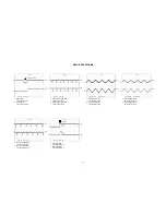
Page 15: ...9 DAC output L ch JH connector pin 9 0 DAC output R ch JH connector pin 8 A Sound signal L ch JK connector pin 4 B Sound signal R ch JK connector pin 5 7 RS signal PA4 JJ connector pin 4 8 R W signal PA5 JJ connector pin 5 1 2 CH1 CH2 3 4 CH1 CH2 5 6 CH1 CH2 7 8 CH1 CH2 9 0 CH1 CH2 A B CH1 CH2 0 5 s 20 ms 50 µs 0 5 s 1 ms 1 ms CH1 5 V CH2 5 V CH1 5 V CH2 5 V CH1 5 V CH2 5 V CH1 5 V CH2 5 V CH1 50 ...

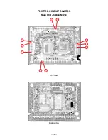
Page 16: ... 14 PRINTED CIRCUIT BOARDS Main PCB JCM454 MA1M Top View Bottom View 2 10 9 3 8 1 4 7 5 6 ...

Page 17: ... 15 Sub PCB KDM454 MA2M 12 11 ...

Page 18: ... 16 LCD PCB JCM454 LCD1M A Top View Bottom View ...

Page 19: ... 17 SCHEMATIC DIAGRAMS Main PCB JCM454 MA1M 2 10 6 6 3 4 1 5 6 9 ...

Page 20: ... 18 Sub PCB KDM454 MA2M 12 11 ...

Page 21: ... 19 Display PCB JCM454 LCD1M ...

Page 22: ... 20 Keyboard PCBs JCM617T KY1M KY2M ...

Page 23: ... 21 PCBs JCM454 CN1M JCM454 CN2M JCM454 CN3M JCM454 CN4M ...

Page 24: ... S8 S9 S10 S11 S12 S13 S14 S15 S16 S17 S18 S19 S20 S21 S22 S23 S24 S25 S26 S27 S28 S29 S30 S31 S32 S33 S34 S35 S36 S37 S38 S39 S40 C1 C2 C3 C4 C5 C6 C7 C12 S17 S8 S9 S10 S32 C9 S33 S34 S35 S36 S37 S38 S39 S40 S3 C12 S2 S1 S11 C9 S12 C16 S29 C15 C14 C13 S30 S31 S32 C12 C11 C10 S20 C9 S19 S18 C13 C14 C15 C16 C10 C12 S21 C11 S1 NC NC NC NC NC NC NC C13 C15 C16 C14 NC NC NC NC NC NC NC NC NC A ...

Page 25: ... S36 S37 S38 S39 S40 C1 C2 C3 C4 C5 C6 C7 C12 S17 S8 S9 S10 S32 C9 S33 S34 S35 S36 S37 S38 S39 S40 S3 C12 S2 S1 S11 C9 S12 C16 S29 C15 C14 C13 S30 S31 S32 C12 C11 C10 S20 C9 S19 S18 C13 C14 C15 C16 C10 C12 S21 C11 S1 NC NC NC NC NC NC NC C13 C15 C16 C14 NC NC NC NC NC NC NC NC NC 125 0 0 2 66 0 0 2 9 087 0 4 5 5 0 4 0 5 0 4 0 15 0 2 0 2 0 4 0 4 0 4 0 4 ...

Page 26: ... 24 EXPLODED VIEW 1 2 3 4 5 6 7 8 9 10 11 12 13 14 15 16 17 18 14 18 17 19 20 21 22 23 24 25 26 27 28 29 R 1 R 2 R 3 ...

Page 27: ... our spare parts department if you need these parts for refurbish 1 Prices and specifications are subject to change with out prior notice 2 As for spare parts order and supply refer to the GUIDEBOOK for Spare parts Supply published seperately 3 The numbers in item column correspond to the same numbers in drawing PARTS LIST CTK 631 ...

Page 28: ...1 3501 7049 JACK POWER HEC2305 01 330 1 AC A J302 3612 0665 JACK PHONE YKB21 5006 1 AG B J303 3612 0789 JACK YKB21 5010 1 AC B J304 3501 4816 JACK DIN YKF51 5051 1 AH B DISPLAY PCB N 3 6927 4380 PCB ASSY LCD1M M240993 1 1 DL B LSI501 2012 6018 LSI LCD DRIVER SED1278F2A 1 AV A D501 2360 3056 DIODE ZENER HZS6A2LTD 1 AA A D502 2390 1344 DIODE 1SS133T 77 1 AA A Q501 502 2253 0710 TRANSISTOR 2SD965 R T...

Page 29: ...19 6927 5090 RUBBER BUTTON M240971 1 1 AE B N 20 6927 4700 RUBBER BUTTON M240942 1 1 AR B N 21 6927 4710 RUBBER BUTTON M240943 1 1 AP B N 22 6927 4720 RUBBER BUTTON M240944 1 1 AR B N 23 6927 5100 RUBBER BUTTON M240945 1 1 AS B N 24 6927 5110 RUBBER BUTTON M240946 1 1 AI B N 25 6927 5120 RUBBER BUTTON M240947 1 1 AI B 26 6927 0510 SWITCH SLIDE KNOB CSB 08D 1 AD B 27 6921 5030 KNOB SLIDE M311859 1 ...

Page 30: ...CASIO TECHNO CO LTD Overseas Service Division Nishi Shinjuku Kimuraya Bldg 1F 5 25 Nishi Shinjuku 7 Chome Shinjuku ku Tokyo 160 0023 Japan ...

Reviews: