— 9 —
1Y
1A
2A
2Y
2G-
1G-
TC74LCX240
AAAA
AAAA
AAAA
A
A
A
A
A
A
A
A
TOUCH PANEL
Y1
Y2
X2
TYU
TXR
TYD
TXL
X1
1
2
3
4
5
6
7
8
9
10
20
19
18
17
16
15
14
13
12
11
VDD
EO
C
DB3
CK
STC
DB4
DB5
NC1
DB6
DB7
OV
F
VSS
AI
N
DB2
NC2
DB1
DB0
OE
VREF
AG
ND
IC82 TC35093
ADCH
ADSTOB
ADSTBY
OCLK
VDD
CS8B
DB3
DB2
DB1
DB0
DB7
DB6
DB5
DB4
CPU
HD62119A03
KO7(TABYG)
KO8(TABXG)
KO6(TABLUB)
KO5(TABRDB)
TC74HC4066
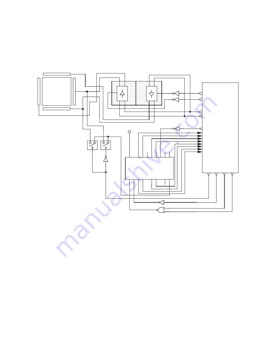
TOUCH PANEL CIRCUIT
Four electrodes are installed in top and bottom right and left of panel, and the touch panel recognizes the
coordinate which was pushed with a pen on panel by detecting change volume of current which flowed through
panel by pushing panel.
Circuit Operation
TXL and TYU of drive signals are sent through LS240 from CPU by X1,Y1 of touch panel when turn on power
supply. And, TXR,TYD signals are output through LS240 from touch panel to AIN terminal of A/D converter
TC35093, and convert the analog value into digital value, and TC35093 outputs digital data DB0~DB7 of 8 bits
to CPU.
TC35093 changes TXR of X axis signal, TYD of Y axis signal in alternating by analog switch 4066 by ADCH
signal from CPU to output digital data, and input analog data into AIN terminal of TC35093.
Synchronize analog data input from AIN terminal in clock signal of 1 pin, and TC35093 outputs digital data
DB0~DB7 to CPU when OE and STC signal input become H.
Summary of Contents for NX-4000
Page 1: ...NX 4000 6000 R without price SEP 1995 INDEX ...
Page 18: ... 17 SCHEMATIC DIAGRAMS Z850 1 PCB ASS Y MAIN BLOCK ...
Page 19: ... 18 Z850 1 PCB ASS Y A D BLOCK ...
Page 20: ... 19 Z850 1 PCB ASS Y DISPLAY BLOCK ...
Page 21: ... 20 Z850 1 PCB ASS Y MEMORY BLOCK ...
Page 26: ...8 11 10 Nishi Shinjuku Shinjuku ku Tokyo 160 Japan Telephone 03 3347 4926 ...


