— 61 —
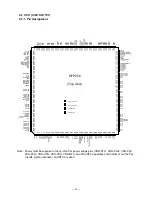
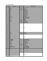
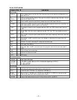
PIN NAME
I/O
DESCRIPTION
AD [31:0]
C/
~BE [3:0]
PAR
~FRAME
~TRDY
~IRDY
~STOP
~DEVSEL
IDSEL
CLK
~RST
~REQ
~GNT
~INTA
I/O
I/O
I/O
I/O
I/O
I/O
I/O
I/O
I
I
I
O
I
O
PCI multiplexed Address and Data Bus. A bus transaction consists of an address cycle followed by one or
more data cycles.
PCI Bus Command and Byte Enables. These signals carry the bus command during the address cycle and
byte enable during data cycles.
Parity. asserts this signal to verify even parity across AD [31:0] and C/~BE [3:0].
Cycle Frame. asserts this signal to indicate the beginning and duration of a bus transaction. It is
de-asserted during the final data cycle of a bus transaction.
Target Ready. A bus data cycle is completed when both ~IRDY and ~TRDY are asserted on the same
cycle.
Initiator Ready. A bus data cycle is completed when both ~IRDY and ~TRDY are asserted on the same
cycle.
Stop. asserts this signal to indicate that the current target is requesting the master to stop current
transaction.
Device Select. asserts this signal when it decodes its addresses as the target of the current
transaction.
ID Select. This input is used during PCI configuration read/write cycles.
PCI System Clock, 33 MHz.
PCI System Reset. asserts this signal to force registers and state machines to initial default
values
PCI Bus Request (bus master mode)
PCI Bus Grant (bus master mode)
PCI Interrupt
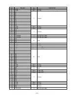
Host Interface
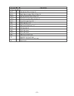
Power Down Interface
~PDOWN
~CLKRUN/
ACTIVITY
I
O
Power down mode enable
~CLKRUN or Memory and I/O activity detection depending on SCR18 [7]
0 = select ~CLKRUN
1 = select ACTIVITY
Clock Interface
REFCLK
CKIN
MCKIN/
LVDSCLK
~EXCKEN
I
I
I/O
I
32 KHz refresh clock source for power down or PALCLK for PALTV
14.318 MHz clock (~EXCKEN = 1) or Video Clock (~EXCKEN = 0)
Memory Clock In (~EXCKEN = 0) or LVDSCLK Out (~ESCKEN = 1), LVDSCLK is a free running clock
which can be used to drive LVDS transmitter for DSTN panels.
External Clock Enable. Select external VCLK form CKIN and MCLK from MCKIN.
8-10-2. Pin Function
Summary of Contents for QT-6100
Page 1: ...SERVICE MANUAL ELECTRONIC CASH REGISTER without price QT 6100 EX 819 AUG 2008 QT 6100 ...
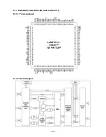
Page 67: ... 65 8 11 ETHERNET CONTROLLER IC28 LAN91C113 8 11 1 Pin Assignment 8 11 2 Block Diagram ...
Page 92: ... 90 11 PCB LAYOUT MAIN PCB E819 1 PCB TOP VIEW ...
Page 93: ... 91 MAIN PCB E819 1 PCB BOTTOM VIEW ...
Page 94: ... 92 INTERFACE PCB E819 S1 PCB TOP VIEW BOTTOM VIEW LED PCB E820 LED PCB TOP VIEW BOTTOM VIEW ...
Page 108: ... 106 Model Name Board No Drawing No CASIO COMPUTER CO LTD QT 6100 EX 819 E820 LED LED ...
Page 120: ... 118 EXPLODED VIEW QT 6060D 2 11 17 14 15 20 Sales Option 16 5 6 12 13 18 19 8 7 10 3 1 4 9 5 ...
Page 135: ... 133 18 DRAWER DL 3616 ...
Page 137: ... 135 19 DRAWER DL 3617 ...

