background image

— 102 —

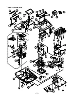
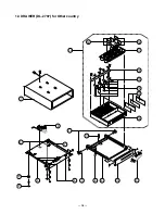
1

4

. DRAWER (DL-2799) for UK, Canada

12

17

11

8

7

6

9

10

1

18

19

5

4

2

5

16

13

15

14

3

Summary of Contents for TE-2200

Page 1: ...SERVICE MANUAL ELECTRONIC CASH REGISTER without price TE 2200 2400 EX 443 544 AUG 2005 TE 2400 TE 2200 Ver 2 Aug 2009 ...

Page 2: ...lfunctions caused by the weak batteries charge the memory protection batteries for over 12 hours before installation or after a long time vacation over 30 days Before installation initialize the terminal and leave it turn on over 12 hours After a long time vacation initialize the terminal and restore the program data if the terminal is in malfunction and leave it turn on over 12 hours Over 48 hour...

Page 3: ... 25 C Auto calendar Effective until 2099 A D Operating temperature 0 C 40 C Operating humidity 10 95 Storage temperature 25 C 65 C Storage humidity 10 95 Vibration strength 1 5 G The machine must be in the carton box 1 3 Main components CPU Name uPD784215AGC279 Number of control bit 16 bit RAM US Name M68AF128BM70 2 Capacity 1 Mbit RAM EURO Name M68AF511AM70 Capacity 4 Mbit Flash ROM Name MBM29F16...

Page 4: ...0 000 hours Backlight 20 000 hours 1 4 Duration of Life Type Drawer Name Specification B D C BU L M DL 2429 D 24H2C B55SRM 9 M DL 2797 D 24H2C B84RM 9 M DL 2798 D 24H2C B84SRM 9 M DL 2799 D 24H2C A84SRM 9 Note Country code B Europe D England C U S A BU Other countries L Canada ...

Page 5: ...B Length 5m Common Slip printer AC adaptor 31AD U or E U 120V E 230V Local purchase Handy scnner HHS 15 Com2 port only Local purchase Handy scnner HS1250 Com2 port only Local purchase Handy scanner Quic Scan 6000 Com2 port only Common CF Memory Card SDCFB xx 505 Local purchase Modem 56k V92 External Local purchase Faxmodem Modem 56k Faxmodem Local purchase Conversion Kit CVK S3 M CVK L3 M Common R...

Page 6: ...ld down JOURNAL FEED 3 Turn the mode switch to PGM position 4 Release JOURNAL FEED You should see 0000000000 on the display If 10 zeros are not shown or another character are shown immediately set the mode switch to OFF and restart from the beginning of this procedure 5 Enter 11 digit program code from the worksheet 6 Press SUBTOTAL to register the program code Wait until beep twice 7 Press SUBTOT...

Page 7: ...nnn 0002 98 2000 Mode symbol date time Clerk descriptor Mc No consecutive No INIT symbol Copyright Model name ROM version ROM label ROM version ROM label Initialization code I O parameter table record No error code Description Choice Program code Print password of PGM mode when flag clear operation is performed Password in PGM3 7 mode Messages and descriptors are written in English 0 French 1 Span...

Page 8: ...nother character are shown immediately set the mode switch to OFF and restart from the beginning of this procedure 5 Press SUBTOTAL to complete Note After flag clear clerk 1 is assigned automatically So do not program clerk 1 as not assignable or not operable in PGM mode Init 2 operation 1 Plug the power cord into an AC outlet 2 Hold down RECEIPT FEED 3 Turn the mode switch to PGM position 4 Relea...

Page 9: ... 7 3 DISASSEMBLY UPPER COVER 1 Remove the printer cover 2 Remove two screws 3 Remove the printer cover 4 Remove two FPCs FPC 10pin FPC 12pin Hooks ...

Page 10: ... 8 5 Remove the screw 6 Remove the upper case by sliding it forward 7 Remove two connectors CN13 CN15 CN13 CN15 8 Remove the UPPER COVER ...

Page 11: ...rews TE 2400 Remove eight screws 10 Remove the FPC 11 Removethe chassis 12 Removethe FPC sheet 13 Removethe spacer 14 Removethe sheet 15 Remove eight screws 16 Remove the KEY frame TE 2200 TE 2400 TE 2400 TE 2200 Chassis FPC sheet Spacer Sheet ...

Page 12: ...W PCB MODE KEY 17 Remove three screws 18 Remove the TACT SW PCB E443 E6 PCB 19 Remove the screw 20 Remove the MODE KEY BACKUP BATTERY 21 Remove the connector 22 Remove the backup battery E443 E6 PCB MODE KEY CN14 ...

Page 13: ...ove four connectors Connector CN7 Connector CN1 Connector CN16 Connector CN5 24 Remove three FPCs FPC CN8 FPC CN9 FPC CN12 NOTE While fixing be fully care to the direction of the FPC Pattern Pattern 25 Remove eight screws ...

Page 14: ... 12 LCD ASS Y 26 Remove five screws and then the LCD ASS Y 27 Remove three screws and one connector PRINTER 28 Remove two E272 PR PCBs 29 Remove four FPCs E272 PR PCB ...

Page 15: ... 13 30 Remove four screws 31 Remove two printer units 32 Remove the battery cover 33 Remove four screws 34 Remove the lower case ...

Page 16: ... 14 DRAWER 35 Remove the case 36 Remove 10 screws 37 Remove the DARWER cable ...

Page 17: ... 15 38 Remove the Bottom plate 39 Loosen 4 screws 40 Remove the screw and then fix the drawer case ...

Page 18: ... 16 POWER SUPPLY 28 Remove the two screws 29 Remove the POWER UPPER CASE 30 Remove three screws 31 Remove the POWER UNIT ...

Page 19: ...i f RS 232C COM1 RS 232C COM2 Drawer Slip printer SP 1300 MODEM or PC CPU RAM Flash Memory Main Display Note Shadowed device and dot line indicate option devices PRT CB 8A 8B PRT CB 8C PRL CB 2 Power supply External printer UP 360 Power supply 31AD U E CF card Journal printer Receipt printer Popup display Multi drawer kit MDL 12 ...

Page 20: ... 16Mbit optional POWER SUPPLY UNIT Transformer Optional MODEM PC Optional Hand Held Scanner HHS 15 5V supply signal only COM1 COM2 optional voltage selector LiB Battery Feed Motor PWB E272 PR PWB E272 PR Feed Motor PWB E443 E22 16Mbit 4Mbit FROM Thermal PRN UNIT Receipt Journal Winder Motor MODE KEY PWB E475 E3 CPU SRAM FPC PWB E443 LCD TE 2200 STROKE or TE 2400 FLAT 16Mbit 1Mbit FROM CPU SRAM 1Mb...

Page 21: ... 19 4 3 RESET CIRCUIT The reset circuit is as follows 4 4 POWER SUPPLY CIRCUIT The power supply circuit is as follows IC32 32pin ...

Page 22: ... 20 4 5 DRAWER I F CIRCUIT The drawer open circuit is as follows ...

Page 23: ... 21 4 6 PRINTER CONTROL CIRCUIT The printer control circuit is as follows ...

Page 24: ...11 P52 A10 P51 A9 P50 A8 P47 AD7 P46 AD6 P45 AD5 P44 AD4 P43 AD3 P42 AD2 P41 AD1 P40 AD0 P87 A7 P86 A6 P85 A5 P84 A4 P83 A3 P95 P94 P93 P92 P91 P90 TEST V PP P37 EXA P36 TI01 P35 TI00 P34 TI2 P33 TI1 P32 TO2 P31 TO1 P30 TO0 P103 TI8 TO8 P102 TI7 TO7 P101 TI6 TO6 P100 TI5 TO5 V DD P67 ASTB P66 WAIT P65 WR P64 RD P63 A19 P11 ANI1 P12 ANI2 P13 ANI3 P14 ANI4 P15 ANI5 P16 ANI6 P17 ANI7 AV SS P130 ANO0 ...

Page 25: ...TROL A D CONVERTER AVDD AVSS P03 NMI INTP2 PCL BUZ AVREF0 ANI0 ANI7 D A CONVERTER ANO0 AVSS AVREF1 ANO1 78K IV CPU CORE ROM RAM BAUD RATE GENERATOR RxD1 SI1 TxD1 SO1 ASCK1 SCK1 RxD2 SI2 TxD2 SO2 ASCK2 SCK2 SI0 SO0 SCK0 BUS I F UART IOE1 RD ASTB WR WAIT A0 A7 AD0 AD7 A8 A15 A16 A19 PORT1 P10 P17 PORT0 P00 P06 PORT2 P20 P27 PORT3 P30 P37 PORT4 P40 P47 PORT5 P50 P57 PORT6 P60 P67 PORT7 P70 P72 PORT8 ...

Page 26: ...ANI0 26 P11 ANI1 27 P12 ANI2 28 P13 ANI3 29 P14 ANI4 30 P15 ANI5 31 P16 ANI6 32 P17 ANI7 33 AVSS A D CONVERTER D A CONVERTER GND 34 P130 ANO0 35 P131 ANO1 36 AVREF1 Application of Standard Voltage for D A CONVERTER 37 P70 RxD2 SI2 38 P71 TxD2 SO2 39 P72 ASCK2 SCK2 40 P20 RxD1 SI1 41 P21 TxD1 SO1 42 P22 ASCK1 SCK1 43 P23 PCL 44 P24 BUZ 45 P25 SI0 SDA0 46 P26 SO0 47 P27 SCK0 SCL0 48 P80 A0 49 P81 A1...

Page 27: ... 75 P62 A18 76 P63 A19 77 P64 RD 78 P65 WR 79 P66 WAIT 80 P67 ASTB 81 VDD Power Supply 82 P100 TI5 TO5 83 P101 TI6 TO6 84 P102 TI7 TO7 85 P103 TI8 TO8 86 P30 TO0 87 P31 TO1 88 P32 TO2 89 P33 TI1 90 P34 TI2 91 P35 TI00 92 P36 TI01 93 P37 EXA 94 TEST VPP TEST pin 95 P90 96 P91 97 P92 98 P93 99 P94 100 P95 IO 8 bit input output PORT IO 8 bit input output PORT IO 8 bit input output PORT IO 8 bit input...

Page 28: ...n Function 4 8 3 Block Diagram A0 A18 Address Inputs DQ0 DQ7 Data Input Output E Chip Enable G Output Enable W Write Enable VCC Supply Voltage VSS Ground ROW DECODER A8 A18 DQ0 DQ7 COLUMN DECODER I O CIRCUITS A0 A7 W G MEMORY ARRAY E VCC VSS 19 A0 A18 W DQ0 DQ7 VCC G VSS 8 E ...

Page 29: ...ction 4 9 3 Block Diagram A0 A16 Address Inputs DQ0 DQ7 Data Input Output E1 E2 Chip Enable G Output Enable W Write Enable VCC Supply Voltage VSS Ground ROW DECODER A7 A16 DQ0 DQ7 COLUMN DECODER I O CIRCUITS A0 A6 W G MEMORY ARRAY VCC VSS E2 E1 17 A0 A16 W DQ0 DQ7 VCC VSS 8 E1 G E2 ...

Page 30: ... to A18 OE DQ0 to DQ15 BYTE RESET STB STB Erase Voltage Generator State Control Command Register Program Voltage Generator Input Output Buffers Data Latch Chip Enable Output Enable Logic Low VCC Detector Timer for Program Erase Address Latch Y Decoder X Decoder Y Gating Cell Matrix RY BY RY BY Buffer Pin Function A 1 A0 to A19 Address Inputs DQ0 to DQ15 Data Inputs Outputs CE Chip Enable OE Output...

Page 31: ... printing the version The version of DIAG and MADK ROM IOC are printed immediately after entering the DIAG mode However DIAG IOC version printing function is available only in QA DIA module All test results are printed by the built in printer receipt 5 3 Notes for the DIAG All test result are printed by the built in receipt printer Make sure to test HHS 15 by connecting to COM2 To perform the cont...

Page 32: ...llows As for tact switch the pressed LED will be lit Mode display 1 PGM 2 RF 3 REG1 4 REG2 5 X 6 Z 7 XZ2 8 OFF Receipt head Off Head down On Head up Journal head Off Head down On Head up No receipt paper Off Paper available On No paper No journal paper Off Paper available On No paper CF CARD sensor Off Not yet inserted On Inserted Drawer 1 sensor Off CLOSE On OPEN Drawer 2 sensor Off CLOSE On OPEN...

Page 33: ...est c0121 39 14 Pop up display test 221 39 15 LCD test n321 40 16 LCD CONTRAST ADJUSTMENT 421 41 17 Display test repeat 521 42 18 Internal printer print test cn03d 43 19 Internal printer graphic print test P1P1P1P2P2P2n13d 44 20 Internal printer dot rate test pn33d 45 21 Internal printer print value test 435 46 22 Internal printer print density test x0235 46 23 COM RS232C test xn04d 47 24 COM RS23...

Page 34: ... B B B B B B B B B B B B B B D A T E 0 5 1 2 3 1 T I M E 2 3 5 9 3 0 D RW 1 O K E N D 1 Print Test See RAM test if ERROR appears while performing the RAM test Operation Operation 2 SUBTOTAL The following tests are performed automatically 1 Display test Refer to 12 Display test Press any key to go to the next test Same in the backlight test also Press any key to go on to the next test Same in the b...

Page 35: ... the test press C key Print The result of all area for RAM test is printed as follows Pop up display A counter is displayed for Pop up display D I A G 0 0 1 1 0 0 n n 0 1 2 3 2 3 Main display n 0 1 2 3 2 3 The result is printed as follows if the test ended with an error If an error occurs while checking the BANKO address 0x60400 for normal RAM n R A M 1 1 R A M WR O K E N D 1 1 Print NG RAM WR NG ...

Page 36: ... 1 1 0 0 n n 0 1 2 3 Print The result for all area test for RAM is printed as follows Refer to RAM WRITE READ test when NG is printed R A M 1 1 1 R A M R D O K E N D 1 1 1 5 CF CARD WRITE READ test Function This test will check the write read test connection test for CF CARD Perform the CF CARD clear test before start of this test Note that this test does not ensure the data inside the CF CARD as ...

Page 37: ...er by rotating the key PRINT NG and the address are printed if READ cannot be done normally C F C A R D 1 1 3 C F R D O K E N D 1 1 3 7 CF CARD CLEAR test Function This test will check the clear test for CF CARD Note that this test does not ensure the data inside the CF CARD as well as its performance Operation Operation 0 n 2 1 3 SUBTOTAL n 0 One time check can be omitted not 0 Continuous check T...

Page 38: ... if WRITE cannot be done normally C F C A R D 3 1 3 C F C L R WR O K E N D 3 1 3 9 Locale information write Function The Locale information is written into FLASH MEMORY Operation Operation x1 x2 0 0 1 6 SUBTOTAL x1 xcountry code x2 SUB CODE x1 x2 10 R Europe 20 R US 30 R UK 40 R Germany 50 R Canada 60 R Direct 61 R Direct Hebrew PRINT The following receipt is not issued when commands other than x1...

Page 39: ...e power by rotating the key to stop this test PRINT The address is not printed when the error occurs C G 1 7 C G R D O K E N D 1 7 NG is printed if CHECK SUM value is not normal 11 FLASH USER AREA clear test Function Clear the area of LOCALE CONTRAST setting Operation Operation 2 1 2 SUBTOTAL PRINT NG is printed if the test is not done correctly R OM 2 1 2 R OM C L R O K E N D 2 1 2 ...

Page 40: ...on n 0 2 1 SUBTOTAL n 0 One time check can be omitted not 0 Continuous check To stop the test press C key Any key must be pressed to end the test when performing one time check PRINT Press any key Press any key 8 8 8 8 8 8 8 8 3 4 5 6 7 8 9 0 D I A G 1 8 8 8 8 8 8 8 8 8 8 A B C D E F G H I J K L M N O P Q R S T U VWX Y Z a b c d e f 1 2 3 4 5 6 7 8 9 0 D I S P 2 1 D I S P O K E N D 2 1 ...

Page 41: ...eys White Green Red 1 OFF 2 White 3 Green 4 White Green PRINT When inputting 0 or without inputting in C 121 is printed When inputting numbers 1 to 4 in C the number input on C and 0120 are printed as the figure shown B A C K L I G H T 1 2 1 B A C K L I G H T O K E N D 1 2 1 B A C K L I G H T c 0 1 2 1 B A C K L I G H T O K E N D c 0 1 2 1 3 4 5 6 7 8 9 0 D I A G 2 2 1 1 2 3 4 5 6 7 8 9 0 Pop up d...

Page 42: ...e power Continuous check turn off the power Operation Operation n 3 2 1 SUBTOTAL n 0 One time check can be omitted not 0 Continuous check To stop the test press C key After the test pattern 4 is displayed until any key is depressed PRINT Press any key Press any key 3 4 5 6 7 8 9 0 A B C D E F G H I J K L M N O P Q R S T U VWX Y Z a b c d e f 1 2 3 4 5 6 7 8 9 0 Press any key Press any key 7 6 5 4 ...

Page 43: ...ns as follows to operate DARK button contrast 1 LIGHT button contrast 1 CA AMT TEND button Contrast determination Write into Flash Contrast adjustment is completed C button Stop adjusting Turn off the power Stop adjusting Pop up display Main display PRINT 3 4 5 X X XX is the setting value A B C D E F G H I J K L M N O P Q R S T U VWX Y Z a b c d e f 1 2 3 4 5 XX XX is the setting value D I S P 4 2...

Page 44: ...Input command Pattern 1 Pattern 2 End Operation Operation 5 2 1 SUBTOTAL Press C key or turn off the power to stop the test PRINT Press any key Press any key 8 8 8 8 8 8 8 8 3 4 5 6 7 8 9 0 D I A G 1 8 8 8 8 8 8 8 8 8 8 A B C D E F G H I J K L M N O P Q R S T U VWX Y Z a b c d e f 1 2 3 4 5 6 7 8 9 0 D I S P 5 2 1 D I S P O K E N D 5 2 1 ...

Page 45: ...he power by rotating the key d 3 prints only receipt 4 prints only journal 5 prints both receipt journal prints alternately Print 1 prints character B 2 prints all characters The printing order is in the order of the character code The characters from 0x20 SP to 0xFA are printed A space is printed for a code without the printing character A character which cannot be printed is a character within t...

Page 46: ...e print images are as follows Graphic pattern 1 Graphic pattern 2 Graphic pattern 1 Graphic pattern 2 repeat for 28 Dot line Print patterns and commands 1Receipt 25 pattern continuous 0 8 5 0 0 0 1 1 3 3 SUBTOTAL The display unit of the print pattern image in the right is as follows Horizontal dot Vertical do line 2Receipt 50 pattern continuous 0 8 5 1 7 0 1 1 3 3 SUBTOTAL The display unit of the ...

Page 47: ...e line are printed in all dots 3 dot lines printed in all dots 11 dot lines no printing 3 dot lines printed in all dots 11 dot lines no printing 2 5 dot lines The first 3 dot lines in the 1 2 line 14 dot lines out of one line are printed in all dots 5 dot lines printed in all dots 9 dot lines no printing 5 dot lines printed in all dots 9 dot lines no printing 3 7 dot lines The first 3 dot lines in...

Page 48: ...int No print 21 Internal printer print value test Function Printing is performed to the internal printer receipt journal according to the following print format This test is performed only once Operation Operation 4 3 5 SUBTOTAL Print 7 dot line black printing one line feed Character codes from 0x30 to 0x7c are printed for 3 lines Receipt side cut Journal side Feeds to the cut position of the rece...

Page 49: ... D T R 1 1 C D 1 0 O K D T R 1 1 C I 1 0 O K R T S 1 0 C T S 1 0 O K D T R 1 0 D S R 1 0 O K D T R 1 0 C D 1 0 O K D T R 1 0 C I 1 0 O K T x D R x D O K E N D 4 1 x 0 d 1 C OM 1 x n 0 4 1 R T S 1 1 C T S 1 0 O K D T R 1 1 D S R 1 0 O K D T R 1 1 C D 1 0 O K D T R 1 1 C I 1 0 O K R T S 1 0 C T S 1 0 O K D T R 1 0 D S R 1 0 O K D T R 1 0 C D 1 0 O K D T R 1 0 C I 1 0 O K T x D R x D O K E N D x n 0 ...

Page 50: ...t C OM B A T C H 4 0 R T S 1 1 C T S 1 0 O K D T R 1 1 D S R 1 0 O K D T R 1 1 C D 1 0 O K D T R 1 1 C I 1 0 O K R T S 1 0 C T S 1 0 O K D T R 1 0 D S R 1 0 O K D T R 1 0 C D 1 0 O K D T R 1 0 C I 1 0 O K T x D R x D O K R T S 2 1 C T S 2 0 O K D T R 2 1 D S R 2 0 O K R T S 2 0 C T S 2 0 O K D T R 2 0 D S R 2 0 O K T x D R x D O K E N D 4 0 COM 1 test result COM 2 test result Figure RS232C port co...

Page 51: ...To stop the operation press Esc key or turn off the power by rotating the key Press any key to enter the next test a 0 time setting x1 x2 time x3 x4 minutes x5 x6 second 1 time setting x1 x2 year x3 x4 month x5 x6 day The test will be done one time Main display Print Y Y MM D D H H MM S S 1 D A T E T I M E 7 0 E S C E N D 7 0 Date and time setting Date and time display D A T E T I M E Y Y MMD D 0 ...

Page 52: ...ion is displayed after all drawers open while performing continuous check Print D RW 9 1 D RW A L L O K E N D 9 1 D RW 1 0 0 9 1 D RW 1 O K E N D 1 0 0 9 1 x 0 x 1 27 Buzzer test Function This test will check the buzzer function Ring the one shot buzzer Ring the 500msec intermittent buzzer while performing continuous check Press C key or turn off the power to stop the intermittent buzzer Operation...

Page 53: ...play and Main display turn on Repeat printing in the internal printer Operation Operation 1 9 3 SUBTOTAL Press C key or turn off the power to stop Pop up display Main display 8 8 8 8 8 8 8 8 D I A G 1 9 3 8 8 8 8 8 8 8 8 8 8 Print pattern image Print Prints only in the receipt of the internal printer with 50 dot rate ...

Page 54: ...y zz key code type Main display xxx hard key code zz key code type Print No printing is done in this test Location of the hard key code x 8 8 8 8 8 z z D I A G 9 4 x x x z z TE 2200 071 064 062 060 054 048 042 036 030 024 018 081 076 070 065 063 061 059 053 047 041 035 029 023 017 080 075 069 058 052 046 040 034 028 022 015 079 074 068 057 051 045 039 033 027 014 016 078 073 067 056 050 044 038 03...

Page 55: ...77 084 091 098 105 021 017 034 041 048 055 062 069 076 083 090 097 104 020 015 033 040 047 054 061 068 075 082 089 096 103 014 016 032 039 046 053 060 067 074 081 088 095 102 011 012 013 C 7 8 9 4 5 6 1 2 3 0 RECEIPT FEED JOURNAL FEED 109 110 111 114 115 116 117 118 119 112 113 TE 2400 for US 045 052 059 066 073 080 087 094 101 108 038 036 033 030 044 051 058 065 072 079 086 093 100 107 037 035 03...

Page 56: ...ge Display with three digits Example 300 indicates 3 00 v Operation Operation 9 6 SUBTOTAL Press C key or turn off the power to stop the test Pop up display xxx battery voltage Main display xxx battery voltage Print No printing in this test x 8 8 8 8 x x x D I A G 9 6 x x x ...

Page 57: ...wo consecutive transactions attempted in the refund mode Attemptmadetoregisteranitemwithoutinputting a check number Attemptmadetoregisteranitemwithoutinputting a table number Finalize operation attempted without entering the number of customer No department linked PLU is registered Actual stock quantity becomes less than the minimum stock quantity Actual stock quantity becomes is negative No condi...

Page 58: ... E049 E050 E051 E052 E053 E054 E055 E056 E059 E060 E061 E062 E064 E066 E075 E085 E100 E101 E103 E105 E106 E112 Print Cheque Print Check Endorsement REG buffer full Print bill Insert slip paper and retry CHECK memory full DETAIL memory full CHK TBL No is occupied CHK TBLNo isbusy CHK TBL No is not opened Out of CHK TBL No range In the SEP CHK operation CHK range full Press EAT IN or TAKEOUT key Pri...

Page 59: ... the employee who is not clocked in Attempttoclockintheemployeewhohasclocked in already Time and attendance file becomes full No CF card is set Illegally formatted CF card The designated file is not found in the CF card Insufficient memory in the CF card Cannotwrite becausedesignatedfilehasalready been Insert new slip paper Close the receipt platen arm Enter proper minus coupon amount Set the arra...

Page 60: ... error 2019 No response 2020 File not found 2021 File create error 2022 File I O error 2023 Retry error 2024 Receive SYN error 2025 Receive FIN error 2026 FIN is in sending sequence whole recalling n_write 2027 Illegal format 2028 Illegal command 2029 Busy with response 2030 Communication abortion 2031 Online receiving hardware error 2032 Inline receiving hardware error 2033 Online receiving overr...

Page 61: ...IN2 IN2 2ch 15 14 16 12 10 11 13 9 VCC 2 3 1 5 7 6 4 8 VS IN1 IN2 S GND IN3 IN4 VS NC RFG2 OUT4 OUT3 OUT2 OUT1 RFG1 P GND LB1936V IN1 IN2 IN3 IN4 S GND VCC VS P GND RFG2 OUT4 OUT3 VS RFG1 OUT2 OUT1 Stepping Motor 10 uF 10 uF Control and logic circuit Output drive circuit LB1936V 30K 30K 30K 30K 30K 30K 30K 30K ...

Page 62: ...y H L H No Z y auto powerdown feature H high level L low level X irrelevant Z high impedance EACH RECEIVER INPUTS OUTPUTS RIN2 RIN1 RIN3 RIN5 FORCEOFF VALID RIN RS 232 LEVEL ROUT2B ROUT RECEIVER STATUS L X L X L Z Powered off while H X L X H Z ROUT2B is active L L H Yes L H L H H Yes L L Normal operation with H L H Yes H H Normal o eration with auto powerdown di bl d bl d H H H Yes H L disabled en...

Page 63: ... 22 44 43 42 41 40 39 38 37 36 35 34 33 32 31 30 29 28 27 26 25 24 23 NC A18 A17 A7 A6 A5 A4 A3 A2 A1 A0 CE VSS OE D0 D8 D1 D9 D2 D10 D3 D11 NC A19 A8 A9 A10 A11 A12 A13 A14 A15 A16 BYTE VSS D15 A 1 D7 D14 D6 D13 D5 D12 D4 VCC MX23C1610 MODE SELECTION CE OE Byte D15 A 1 D0 D7 D8 D15 Mode Power H X X X High Z High Z Stand by L H X X High Z High Z Active L L H Output D0 D7 D8 D15 Word Active L L L I...

Page 64: ...11 10 8 9 8 SN74LV04 IC19 IC21 9 SN74LV11 IC25 1A 1Y 2A 2Y 1 2 3 4 5 7 6 3A GND 3Y VCC 6A 6Y 5A 5Y 4Y 4A 14 13 12 11 10 8 9 1 2 3 4 5 7 6 VCC 14 13 12 11 10 8 9 1C 1Y 3C 3B 3A 1A GND 1B 2A 2B 2C 2Y 3Y 10 SN74LV139 IC24 1G 1Y0 1Y1 1Y2 1Y3 2Y0 2Y1 2Y2 2Y3 1A 1B 2G 2A 2B 1 2 3 15 14 13 4 5 6 7 12 11 10 9 1 2 3 4 5 6 7 8 16 15 14 13 12 11 10 9 1G 1A 1B 1Y0 1Y1 1Y2 1Y3 GND VCC 2G 2A 2B 2Y0 2Y1 2Y2 2Y3 ...

Page 65: ... 10 1A4 12 2A1 14 2A2 1Y1 3 1Y2 5 1Y3 7 1Y4 9 2Y1 11 2Y2 13 EN 15 2OE 1OE To Three Other Channels 1A1 1Y1 1 2 3 2OE To One Other Channel 2A1 2Y1 15 12 11 13 SN74LV373 IC34 1 20 2 19 3 18 4 17 5 16 6 15 7 14 8 1Q 1D 2Q 2D 3Q 3D 4Q 13 Vcc 8Q 8D 7D 7Q 6D 6Q 5D 9 12 10 4D GND 11 5Q Output Control Enable G Q G OE D D G OE Q Q G OE D D G OE Q D G OE Q Q G OE D D G OE Q Q G OE D 1Q 1D Output Control Enab...

Page 66: ... FUNCTION TABLE 8Q 8D 7D 7Q 6D 6Q 5D 9 12 10 4D GND 11 5Q OE CLK OE INPUTS OUTPUT Q H L Q0 Z CLK D L L L H H L X X L X GND 1B 1Y 2A 2B 2Y 4B 4A 4Y 3B 3A 3Y 1A 1 2 3 4 5 7 6 VCC 14 13 12 11 10 8 9 1 2 3 4 5 6 7 8 16 15 14 13 12 11 10 9 1B 2B 3B 4B 5B 6B 7B E 1C 2C 3C 4C 5C 6C 7C COM 7C 6C 5C 4C 3C 2C 1C COM 7 6 5 4 3 2 1 7B 6B 5B 4B 3B 2B 1B 10 11 12 13 14 15 16 9 ...

Page 67: ... PIN FUNCTION 2 VSS 1 Output 2 3 1 VSS VIN VOUT Current Limit Voltage Reference VIN VOUT VSS 2 3 4 5 6 7 8 9 10 11 12 13 14 15 30 1 29 28 27 26 25 24 23 22 21 20 19 18 17 16 WR D0 D1 D2 D3 D4 D5 D6 D7 CS2 AMC ANDI0 ANDI1 ANDO0 GND VCC C D CS1 S0 SCLK CLK SMC ORO0 ORI1 TEB ORI0 RESET INT A0 LCD_CS ...

Page 68: ... 66 8 PCB LAYOUT MAIN PCB E466 1 PCB TOP VIEW ...

Page 69: ... 67 MAIN PCB E466 1 PCB BOTTOM VIEW ...

Page 70: ... 4 MAIN PCB CIRCUIT 4 7 72 1 5 MAIN PCB CIRCUIT 5 7 73 1 6 MAIN PCB CIRCUIT 6 7 74 1 7 MAIN PCB CIRCUIT 7 7 75 2 TACT SW PCB CIRCUIT 76 3 LCD DISPLAY PCB CIRCUIT 77 4 LED DISPLAY PCB CIRCUIT 78 4 1 LED DISPLAY PCB CIRCUIT 1 2 78 4 2 LED DISPLAY PCB CIRCUIT 2 2 79 5 REAR DISPLAY PCB CIRCUIT 80 6 KEY SHEET SW PCB CIRCUIT TE 2200 81 7 KEY SHEET SW PCB CIRCUIT TE 2400 82 ...

Page 71: ... 69 E443 1 Model Name Board No Drawing No MAIN BOARD 1 7 RJE501624D302 CASIO COMPUTER CO LTD TE 2200 2400 EX 443 544 ...

Page 72: ... 70 E443 1 Model Name Board No Drawing No MAIN BOARD 2 7 RJE501624D302 CASIO COMPUTER CO LTD TE 2200 2400 EX 443 544 ...

Page 73: ... 71 E443 1 Model Name Board No Drawing No MAIN BOARD 3 7 RJE501624D302 CASIO COMPUTER CO LTD TE 2200 2400 EX 443 544 ...

Page 74: ... 72 E443 1 Model Name Board No Drawing No MAIN BOARD 4 7 RJE501624D302 CASIO COMPUTER CO LTD TE 2200 2400 EX 443 544 ...

Page 75: ... 73 E443 1 Model Name Board No Drawing No MAIN BOARD 5 7 RJE501624D302 CASIO COMPUTER CO LTD TE 2200 2400 EX 443 544 ...

Page 76: ... 74 E443 1 Model Name Board No Drawing No MAIN BOARD 6 7 RJE501624D302 CASIO COMPUTER CO LTD TE 2200 2400 EX 443 544 ...

Page 77: ... 75 E443 1 Model Name Board No Drawing No MAIN BOARD 7 7 RJE501624D302 CASIO COMPUTER CO LTD TE 2200 2400 EX 443 544 ...

Page 78: ... 76 E443 E6 Model Name Board No Drawing No TACT SW BOARD RJE501624D305 CASIO COMPUTER CO LTD TE 2200 2400 EX 443 544 ...

Page 79: ... 77 E433 LCD Model Name Board No Drawing No LCD DISPLAY BOARD RJE501624D303 CASIO COMPUTER CO LTD TE 2200 2400 EX 443 544 ...

Page 80: ... 78 E443 LED Model Name Board No Drawing No LED DISPLAY BOARD 1 2 RJE501624D304 CASIO COMPUTER CO LTD TE 2200 2400 EX 443 544 ...

Page 81: ... 79 E443 LED Model Name Board No Drawing No LED DISPLAY BOARD 2 2 RJE501624D304 CASIO COMPUTER CO LTD TE 2200 2400 EX 443 544 ...

Page 82: ... 80 E443 E22 Model Name Board No Drawing No REAR DISPLAY BOARD RJE501624D309 CASIO COMPUTER CO LTD TE 2200 2400 EX 443 544 ...

Page 83: ... 81 E443 E4 Model Name Board No Drawing No KEY SEET STROKE RJE501624D307 CASIO COMPUTER CO LTD TE 2200 EX 443 ...

Page 84: ... 82 E544 E4 Model Name Board No Drawing No KEY SEET FLAT RJE501624D315 CASIO COMPUTER CO LTD TE 2400 EX 544 ...

Page 85: ...IST MODEL TE 2200 2400 EX 442 544 TE 2200 Explode view 84 1 MAIN PCB Block 86 2 Main Display Block 86 3 Rear Display Block 87 4 Keyboard Block 87 5 Power supply Block 88 6 Upper Case Block 88 7 Switch Board Block 88 8 Lower Case Block 88 9 Printer Block 89 10 Others 89 TE 2400 Explode view 90 1 MAIN PCB Block 92 2 Main Display Block 92 3 Rear Display Block 93 4 Keyboard Block 93 5 Power supply Blo...

Page 86: ... 84 TE 2200 EXPLODED VIEW 0 00 2 3 4 5 6 7 8 9 1 4 6 5 74 46 46 71 1 9 43 7 69 65 71 66 64 64 10 11 53 56 55 52 3 2 44 68 67 14 61 48 49 50 70 70 51 76 77 57 12 13 47 54 8 45 60 59 58 75 73 62 80 63 ...

Page 87: ... 85 TE 2200 KEYBOARD BLOCK 0 00 2 3 4 5 6 7 8 9 1 15 17 16 42 41 18 29 31 30 32 33 35 36 37 38 39 34 40 ...

Page 88: ... 2 2 AC B 10005659 IC CMOS SN74LV08APWR 4 4 4 4 4 AB B 10120130 IC CMOS SN74LV11APWR 1 1 1 AC B 10005669 IC CMOS SN74LV139APWR 1 1 1 1 1 AD B 10207634 IC SN74LVC1G08DCKR 1 1 1 1 1 AB B 10005721 IC CMOS SN74LV244APWR 1 1 1 1 1 AF B 10004413 IC MOS SN74LV32APWR 2 2 1 1 2 AB B 10089475 IC SN74LV367APWR 2 2 2 2 2 AE B 10050431 IC CMOS SN74LV373APWR 1 1 1 1 1 AI B 10005662 IC SN74LV374APWR 3 3 3 AF B 1...

Page 89: ...207416 DP mount L RJE501587 001V01 1 1 AG X 3 Rear Display Block 10211985 RDP assy RJE501542 002V01 1 1 1 10211988 RDP assy RJE501542 003V01 1 1 BY 9 10094111 Rear Display case E140466 001V02 1 1 AF X 9 10211989 Rear Display case RJE501565 001V01 1 1 1 AM X 10 10072602 Rear display plate E140465 1 1 1 1 1 1 AF B 11 10204322 E443 E22 assy RJE501484 001V01 1 1 1 1 1 BV A 12 10211991 FFC joiner A RJE...

Page 90: ...02 1 1 1 AV C 50 10225059 FK plate RJE501514 008V02 1 1 AP C 51 10223217 Paper cutter RJE501069 001V01 1 1 1 1 1 AC C 10203349 Lens R RJE501460 001V01 1 1 1 1 1 AB X 10203350 Lens L RJE501461 001V01 1 1 1 1 1 AB X 52 10207408 E6 chassis RJE501453 001V01 1 1 1 1 1 AU X 53 10211505 Mode SW assy E341052 002V01 1 1 1 1 1 AV B 54 10210684 Blind J RJE501566 001V01 1 1 1 1 1 AA X PCB E443 E6 RJE501497D30...

Page 91: ... BP A 72 10110555 Battery Cover RJE500211 002V01 1 1 1 AB B 72 10110554 Battery cover RJE500211 001V01 1 1 AC B 63224499 Battery spring A G55 A42606 1 1 1 AA C 60006091 Battery spring G67 A43656 1 1 1 AA C 60207658 Battery spring B 1G513 P408A 1 1 1 AB C 60207666 Battery spring B 2G514 P409A 1 1 1 AA C 10211983 Battery cable sub assy RJE501491 001V01 1 1 AB C 10 Others 73 10204698 Key set sub ass ...

Page 92: ... 90 TE 2400 EXPLODED VIEW 4 6 5 55 27 27 52 1 9 24 7 50 46 53 47 45 45 10 11 34 37 36 33 3 2 25 49 48 14 42 29 30 31 51 51 32 57 58 38 12 13 28 35 8 26 41 40 39 56 54 43 44 ...

Page 93: ... 91 TE 2400 KEYBOARD BLOCK 16 15 17 18 19 20 21 22 23 ...

Page 94: ...R 2 2 2 2 2 AC B 10005659 IC CMOS SN74LV08APWR 4 4 4 4 4 AB B 10120130 IC CMOS SN74LV11APWR 1 1 1 AC B 10005669 IC CMOS SN74LV139APWR 1 1 1 1 1 AD B 10207634 IC SN74LVC1G08DCKR 1 1 1 1 1 AB B 10005721 IC CMOS SN74LV244APWR 1 1 1 1 1 AF B 10004413 IC MOS SN74LV32APWR 2 2 1 1 2 AB B 10089475 IC SN74LV367APWR 2 2 2 2 2 AE B 10050431 IC CMOS SN74LV373APWR 1 1 1 1 1 AI B 10005662 IC SN74LV374APWR 3 3 3...

Page 95: ...1586 001V01 1 1 AG X 8 10207416 DP mount L RJE501587 001V01 1 1 AG X 3 Rear Display Block 10211985 RDP assy RJE501542 002V01 1 1 1 10211988 RDP assy RJE501542 003V01 1 1 BY 9 10094111 Rear Display case E140466 001V02 1 1 AF X 9 10211989 Rear Display case RJE501565 001V01 1 1 1 AM X 10 10072602 Rear display plate E140465 1 1 1 1 1 1 AF B 11 10204322 E443 E22 assy RJE501484 001V01 1 1 1 1 1 BV A 12 ...

Page 96: ...64 001V01 6 6 6 6 6 AA X DRW cable sub assy RJE501492 2 1 1 1 1 1 C 39 10203347 CF cover RJE501458 001V01 1 1 1 1 1 AQ C 40 10203348 CN cover RJE501459 001V01 1 1 1 1 1 AQ C 41 10207409 CN chassis RJE501473 001V01 1 1 1 1 1 AJ X 42 10210663 FFC cable C RJE501553 003V01 1 1 1 1 1 AZ C 43 10210666 FFC cable D RJE501553 004V01 2 2 2 2 2 AF C 10211518 PCB spacer SPD 3U 4 4 4 4 4 AB X 10121158 Ferrite ...

Page 97: ... 10204699 Key set sub ass y RJE500074 005V02 1 1 1 AT A 55 10079266 Paper spool E341312 1 1 1 1 1 1 AH A 56 10072547 Wind Pulley E240814 1 1 1 1 1 1 AF A 57 10210643 PR cover ass y RJE501544 001V01 1 1 1 1 1 BJ C 58 10080665 Journal cover E341236 1 1 1 1 1 1 AC C Q ty Price Code Europe UK USA Canada Other Countries ...

Page 98: ... 96 11 DRAWER DL 2429 for USA 16 17 18 11 8 6 15 14 19 9 10 1 12 20 21 5 4 2 3 5 13 7 ...

Page 99: ...DR 19B1 2 AF B 8 10201065 EARTH SPRING E412092 001V02 1 AC C 9 10203374 CYLINDER LOCK CL 23 1 AZ B 10 10215645 FRONT PANEL RJE501385 001V02 1 AZ C 11 19064150 RIVET 5X30 1 AA X 12 10192854 BILL COIN CASE ASSY RJE501368 003V01 1 CH C 13 10200509 BILL HOLER SUB ASSY E341290 002V03 5 AC A 14 10079063 BILL HOLDER SPRING E441357 1 5 AA A 15 10194233 BILL HOLDER PLATE E240845 001V02 1 AK X 16 10078757 B...

Page 100: ... 98 12 DRAWER DL 2797 for Other country 7 12 16 11 8 7 6 9 10 1 20 21 5 4 2 5 17 18 19 18 13 15 14 3 ...

Page 101: ...LLER DR 19B1 2 AF B 8 10201065 EARTH SPRING E412092 001V02 1 AC C 9 10203374 CYLINDER LOCK CL 23 1 AZ B 10 10215645 FRONT PANEL RJE501385 001V02 1 AZ C 11 19064150 RIVET 5X30 1 AA X 12 10200516 BILL COIN CASE ASSY RJE501368 004V01 1 BW C 13 10200509 BILL HOLER SUB ASSY E341290 002V03 4 AC A 14 10079063 BILL HOLDER SPRING E441357 1 4 AA A 15 10194233 BILL HOLDER PLATE E240845 001V02 1 AK X 16 10195...

Page 102: ... 100 13 DRAWER DL 2798 for Europe 7 12 16 11 8 7 6 9 10 1 20 21 5 4 2 5 17 18 19 18 13 15 14 3 ...

Page 103: ...R DR 19B1 2 AF B 8 10201065 EARTH SPRING E412092 001V02 1 AC C 9 10203374 CYLINDER LOCK CL 23 1 AZ B 10 10215645 FRONT PANEL RJE501385 001V02 1 AZ C 11 19064150 RIVET 5X30 1 AA X 12 10200516 BILL COIN CASE ASSY RJE501368 004V01 1 BW C 13 10200509 BILL HOLER SUB ASSY E341290 002V03 4 AC A 14 10079063 BILL HOLDER SPRING E441357 1 4 AA A 15 10194233 BILL HOLDER PLATE E240845 001V02 1 AK X 16 10195656...

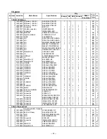
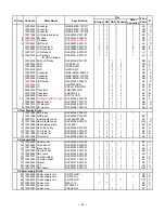
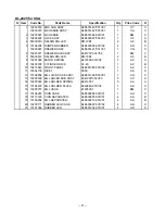
Page 104: ... 102 14 DRAWER DL 2799 for UK Canada 12 17 11 8 7 6 9 10 1 18 19 5 4 2 5 16 13 15 14 3 ...

Page 105: ...341274 002V04 1 BQ C 7 55000619 DELRIN ROLLER DR 19B1 2 AF B 8 10201065 EARTH SPRING E412092 001V02 1 AC C 9 10203374 CYLINDER LOCK CL 23 1 AZ B 10 10215645 FRONT PANEL RJE501385 001V02 1 AZ C 11 19064150 RIVET 5X30 1 AA X 12 10225530 BILL COIN CASE ASSY RJE501368 006V01 1 CH C 13 10200509 BILL HOLER SUB ASSY E341290 002V03 4 AC A 14 10079063 BILL HOLDER SPRING E441357 1 4 AA A 15 10194233 BILL HO...

Page 106: ... COMPUTER CO LTD Overseas Service Division 6 2 Hon machi 1 Chome Shibuya ku Tokyo 151 8543 Japan Ver 1 Aug 2008 Correction of the PARTS LIST P87 and P93 Ver 2 Aug 2009 Correction of the PARTS LIST P84 and 87 ...

Reviews: