Chapter XVIII Working Principle
228
Chapter XVIII Working Principle
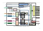
The complete circuits of 4456 Series Digital Phosphor Oscilloscope consist of analog channel, clock and
acquisition circuit, trigger circuit, digital signal processing circuit (data receiving, DPX processing and data
storage), embedded CPU, power supply circuit, logic analyzer module (option 001) and waveform generation
module (option 002). The block diagram of the hardware is shown in Figure 18.1.
The design of the analog channel bandwidth is always the core part of circuit design. During design, it is
necessary to select the appropriate bandwidth of the low noise amplifier and relay switch according to the
bandwidth specifications of different models, thus reducing the cost and system power consumption according to
different bandwidths. Therefore, during the design of the analog channel, the serialization extension of the whole
model is realized by replacing different channels based on the modularization and serialization concepts.
The clock and acquisition circuit mainly consists of a highly stable clock phase-locked loop and a fast ADC. The
clock generator is composed of a frequency synthesizer and a reference clock oscillator. The generated 2.5 GHz
clock signal is divided into two and sent to the two ADCs at the back end as the input clock of the A/D converter.
The 4456C/D uses two ADCs for acquisition upon designing the acquisition circuit. The first ADC collects the
signals of CH1 and CH2 and the second ADC collects the signals of CH3 and CH4. The highest sample rate can
be 5GSa/s when single or dual channels are used simultaneously or 2.5GSa/s when three or four channels are used
simultaneously. The 4456CM/DM uses one ADC for acquisition upon designing the acquisition circuit. The
highest sample rate can be 5GSa/s for a single channel, 2.5GSa/s for dual channels and 1.25GSa/s for three or four
channels used simultaneously.
The trigger circuit includes the analog and digital trigger circuits. The video and external triggers are implemented
by using traditional analog trigger, while the edge, pulse width, pattern, logic and runt triggers are implemented by
using new digital trigger. The digital trigger technology uses the digital signal processing method to perform
trigger point determination against ADC samples collected and detect effective trigger events with an accurate
algorithm. It can accurately display and analyze the measurement signal and has such features as lower trigger
jitter, higher trigger sensitivity, smaller pulse detection width and more accurate channel delay calibration.
The digital signal processing circuit includes high-speed data receiving, deceleration and storage, digital
fluorescent display processing, protocol trigger and analysis and other function units. The processing speed of this
part directly determines the waveform capture rate of the whole instrument. This product uses 2 high-performance
FPGAs, one as the main FPGA and the other as the slave FPGA. The slave FPGA is used to complete data
acquisition and storage, waveform generation, protocol trigger and analysis, and data communication; the main
FPGA is used to complete data acquisition and storage, waveform generation, image synthesis, fluorescent display,
digital trigger, and data communication.
The embedded CPU system is mainly used to complete the control of the whole instrument and the parameter
measurement of waveforms, mathematical operation, FFT spectrum analysis, limit/mask test, and power
measurement. This part also provides rich communication interface functions, including USB main control, USB
device, Ethernet interface, VGA display interface, and reference clock input and output interfaces. The Ethernet
interface enables remote programmable control and can be used to build a distributed system.
The logic analyzer module (option 001) is mainly used for signal acquisition of 16 digital channels. It can be
combined with the oscilloscope module to realize the functions of a mixed signal oscilloscope.
The waveform generator module (option 002) is mainly used for waveform generation of one channel and can
output sine wave, square wave/pulse, triangle/oblique wave, noise signal, and arbitrary waveform.
Summary of Contents for 4456 Series
Page 10: ...VIII...
Page 55: ...Chapter V Trigger System 45 Fig 5 51 RF Test Signal Example...
Page 69: ...Chapter VII Mathematical Operation 59 Fig 7 10 Advanced Math Example...
Page 71: ...Chapter VIII Display System 61 Fig 8 3 Wfm Palette Menu Fig 8 4 Normal Palette...
Page 72: ...Chapter VIII Display System 62 Fig 8 5 Inverted Palette Fig 8 6 Temperature Palette...
Page 75: ...Chapter VIII Display System 65 Fig 8 12 XY Display Example...
Page 165: ...Chapter XI Protocol Analyzer Option 155 Fig 11 242 1553 Trigger and Analysis Example...

