7
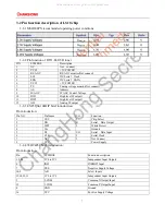
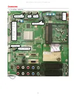
3-2 Pin function description of LS18 chip
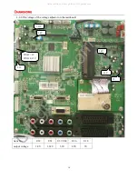
3-2-1 MSD308PX recommended operating power conditons
3-2-2 Pin function of DTI1-E4I1VH tuner
PIN
SYMBOL
Description
1
NC
Not connect
2
VCC2
+5V POWER
3
RF-AGC
RF-AGC monitor(Not connect)
4
SCL
I2C Serial Clock
5
SDA
I2C Serial DATA
6
VCC3
+5V POWER
7
TU
Tuning voltage monitor(Not connect)
8
AS
Address
9
IF-AGC
IF AGC Control Voltage
10
DIF1
High level IF output1
11
DIF2
High level IF output1
12
AIF
Analog IF output
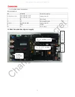
3-2-3 EN25Q64-104HIP brief introduction:
Pin introduction:
Pin NO.
Pin Name
I/O
Function
1
CS#
I
Chip Select
2
DO
O
Serial Data Output
3
WP#
I
White Protect
4
Vss
Ground
5
DI
I/O
Serial Data Input
6
CLK
I
Serial Clock
7
NC
I
Not Connect
8
VCC
Power Supply
3-2-4 74HC4052 brief introduction:
Pin introduction:
Pin
SYMBOL
Function description
1,5,2,4
2Y0 to 2Y3
Independent Input Outputs
6
INH
INHIBIT Input
7
VEE
Negative Supply Voltage
10,9
A,B
Select Inputs
12,14,15,11
1Y0 to 1Y3
Independent Input Outputs
3
2-COM
Common X Output/Input
13
1-COM
Common Y Output/Input
8
GND
Ground
16
VCC
Positive Supply Voltage
All manuals and user guides at all-guides.com


