Copyright CPS America Co., Ltd. Page 31
II) CONFIGURATION:
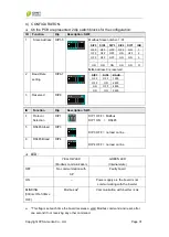
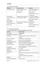
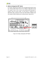
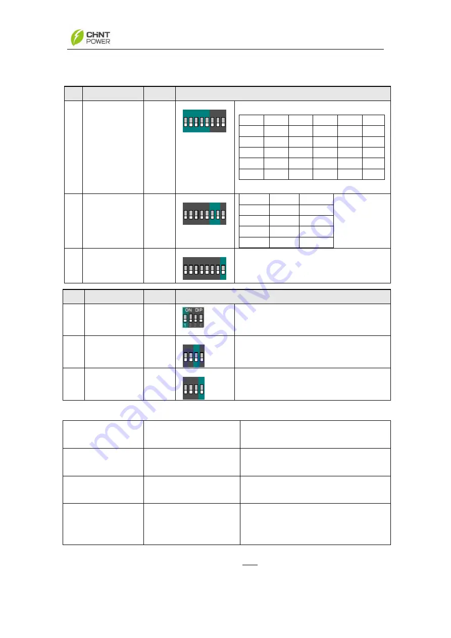
On the PCB are presented 2 dip switch blocks for the configuration:
ID
Function
Dip
Description: SW2
1
Slave Address DIP1-5
1 2 3 4 5
6 7 8
ON
DIP
Modbus Slave number: 1-31
DIP5
DIP4
DIP3
DIP2
DIP1
IND
OFF
OFF
OFF
OFF
ON
1
OFF
OFF
OFF
ON
OFF
2
OFF
OFF
OFF
ON
ON
3
..
..
..
..
..
..
ON
ON
ON
ON
ON
31
N.B.
Address 0 is reserved.
2
Baud Rate
setting
DIP6-7
1 2 3 4 5
6 7
8
ON
DIP
DIP7
DIP6
BAUD
OFF
OFF
1200
OFF
ON
2400
ON
OFF
4800
ON
ON
9600
3
Reserved
DIP8
1 2 3 4 5 6 7 8
ON
DIP
ID
Function
Dip
Description: SW3
4
Protocol
Selection
DIP1
DIP 1 OFF = Modbus
DIP 1 ON = RS485
5
RS485A load
DIP3
1 2
3
4
DIP
ON
DIP 3 OFF = no load on line
DIP 3 ON = 120Ohm load on the line
6
RS485B load
DIP4
1 2 3
4
DIP
ON
DIP 4 OFF = no load on line
DIP 4 ON = 120Ohm load on the line
LED:
YELLOW LED
(Modbus communication)
GREEN LED
(Internal state)
OFF
No communication with
AP
Faulty board
ON
--
Power supply ok, the board is not
communicating with the inverter
BLINKING
(500ms ON- 500ms
OFF)
Modbus ok
2
Communication with inverter is ok
2.
This flag is set each time the board receives a valid Modbus command and reset, after
one second if not receiving any other command.

