CS42528
40
DS586PP5
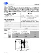
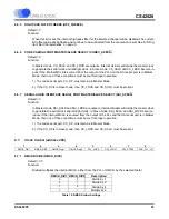
Send stop condition, aborting write.
Send start condition.
Send 10011xx1(chip address & read operation).
Receive acknowledge bit.
Receive byte, contents of selected register.
Send acknowledge bit.
Send stop condition.
Setting the auto increment bit in the MAP allows successive reads or writes of consecutive registers. Each
byte is separated by an acknowledge bit.
4.8
Interrupts
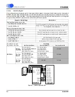
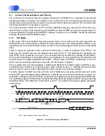
The CS42528 has a comprehensive interrupt capability. The INT output pin is intended to drive the inter-
rupt input pin on the host microcontroller. The INT pin may be set to be active low, active high or active
low with no active pull-up transistor. This last mode is used for active low, wired-OR hook-ups, with mul-
tiple peripherals connected to the microcontroller interrupt input pin.
Many conditions can cause an interrupt, as listed in the interrupt status register descriptions. See “Inter-
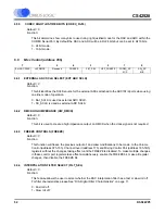
rupt Status (address 20h) (Read Only)” on page 64. Each source may be masked off through mask reg-
ister bits. In addition, each source may be set to rising edge, falling edge, or level sensitive. Combined
with the option of level sensitive or edge sensitive modes within the microcontroller, many different con-
figurations are possible, depending on the needs of the equipment designer.
4.9
Reset and Power-up
Reliable power-up can be accomplished by keeping the device in reset until the power supplies, clocks
and configuration pins are stable. It is also recommended that reset be activated if the analog or digital
supplies drop below the recommended operating condition to prevent power glitch related issues.
When RST is low, the CS42528 enters a low power mode and all internal states are reset, including the
control port and registers, and the outputs are muted. When RST is high, the control port becomes oper-
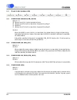
ational and the desired settings should be loaded into the control registers. Writing a 0 to the PDN bit in
the Power Control Register will then cause the part to leave the low power state and begin operation. If
the internal PLL is selected as the clock source, the serial audio outputs will be enabled after the PLL has
settled. See “Power Control (address 02h)” on page 48 for more details.
The delta-sigma modulators settle in a matter of microseconds after the analog section is powered, either
through the application of power or by setting the RST pin high. However, the voltage reference will take
much longer to reach a final value due to the presence of external capacitance on the FILT+ pin. A time
delay of approximately 80ms is required after applying power to the device or after exiting a reset state.
During this voltage reference ramp delay, all serial ports and DAC outputs will be automatically muted.
4.10
Power Supply, Grounding, and PCB layout
As with any high resolution converter, the CS42528 requires careful attention to power supply and ground-
ing arrangements if its potential performance is to be realized. Figure 5 shows the recommended power
arrangements, with VA and VARX connected to clean supplies. VD, which powers the digital circuitry, may
be run from the system logic supply. Alternatively, VD may be powered from the analog supply via a ferrite
bead. In this case, no additional devices should be powered from VD.
For applications where the output of the PLL is required to be low jitter, use a separate, low noise analog
+5 V supply for VARX, decoupled to AGND. In addition, a separate region of analog ground plane around
the FILT+, VQ, LPFLT, REFGND, AGND, VA, VARX, RXP/and RXP0 pins is recommended.


